


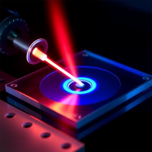
Laser dicing is the backbone of making semiconductor chips, but it comes with an industrial reality: the process must be precise every time. Compared with blade cutting, laser dicing is attractive because it can separate delicate, low-strength materials while reducing mechanical stress. The trade-off is control. Too few laser pulses leave wafer regions only partially cut; too many can damage the substrate or even the tape used to hold it in place. Conventional monitoring approaches often struggle with speed, stability, or robustness on production floors.
A research team led by Professor Hirofumi Hidai at Chiba University has introduced a fast, real-time diagnostic based on a signal that is easy to overlook: recoil force. Recoil force is the tiny reaction produced when a laser rapidly heats and vaporizes material at the wafer surface. By measuring this reaction with high sensitivity, the team aimed to infer how deeply the laser is actually processing the sample.
In laboratory tests, the researchers used nanosecond laser pulses lasting only 25 billionths of a second to drill silicon. During each pulse sequence, they recorded recoil force using a load cell, translating mechanical reaction into a measurable electrical signal. They found systematic trends: recoil force rose with increasing pulse energy, and decreased when the laser focus was defocused away from the wafer surface. These behavior patterns implied an underlying mathematical relationship between recoil force and processing conditions.
The core idea was then turned into a depth monitor. As repeated pulses drilled deeper into the wafer, the recoil force diminished along a predictable curve. At the point of full penetration, the curve shifted noticeably, marking the moment the laser had successfully cut through. This “signature” reduces reliance on post-process inspection and supports in-line feedback without disrupting manufacturing flow.
Prof. Hidai explains that directly measuring recoil enables detection of processing depth and penetration in real time—an advantage for maintaining yield during high-throughput dicing. Using their model, the team also estimated processing depth with a relative error of 24.3%, demonstrating practical utility despite inherent material and system variability.
Beyond validating a new sensing method, the researchers expect impact across precision laser manufacturing. Fewer under- or over-processed wafers could mean fewer defects, more stable chip supply, and lower costs for devices used in smartphones, automobiles, and medical equipment. They also envision integration with laser systems for automatic adjustment of cutting conditions, moving toward smarter, self-optimizing production tools.
The work was made available online on June 8, 2026, and is scheduled to be published in Volume 203 of Optics and Laser Technology on November 1, 2026.
More on Chiba University news can be found here: https://www.cn.chiba-u.jp/en/news/
Keywords
Laser dicing; recoil force sensing; laser ablation; processing depth monitoring; nanosecond pulses; semiconductor manufacturing; real-time diagnostics; load cell measurement; material penetration; yield optimization.
Cite Scienmag News
Bethany Barker. (July 27, 2026). Real-Time Laser Ablation Monitoring Detects Wafer Penetration via Recoil Force. Scienmag. https://scienmag.com/real-time-laser-ablation-monitoring-detects-wafer-penetration-via-recoil-force/
Bethany Barker. "Real-Time Laser Ablation Monitoring Detects Wafer Penetration via Recoil Force." Scienmag, 27 July 2026, https://scienmag.com/real-time-laser-ablation-monitoring-detects-wafer-penetration-via-recoil-force/. Accessed 3 September 2026.
Bethany Barker. "Real-Time Laser Ablation Monitoring Detects Wafer Penetration via Recoil Force." Scienmag. July 27, 2026. https://scienmag.com/real-time-laser-ablation-monitoring-detects-wafer-penetration-via-recoil-force/


