

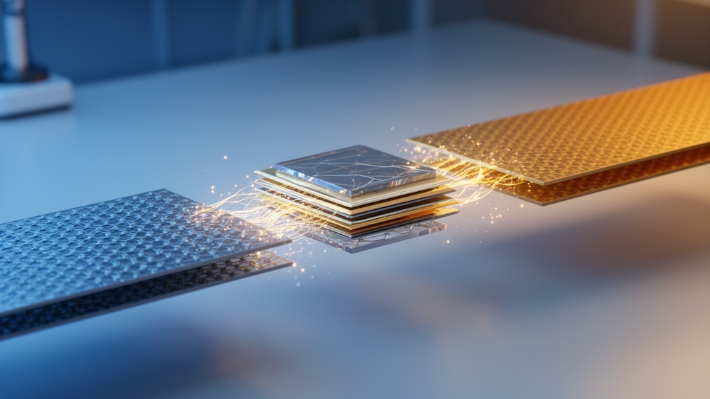
A research team led by the Korea Advanced Institute of Science and Technology has demonstrated that one contact material, tin diselenide, can efficiently inject charge into both p-type and n-type atomically thin semiconductors. The researchers paired the layered material with monolayer tungsten diselenide and monolayer molybdenum disulfide, finding that it enabled distinct tunneling mechanisms at the two interfaces. In p-type WSe₂ devices, the contact increased maximum drive current by more than 1,000 times relative to conventional nickel electrodes.
In n-type MoS₂ devices, it produced steep switching and an on/off current ratio exceeding one billion. The peer-reviewed study, published in Advanced Materials, also yielded a functioning complementary metal-oxide-semiconductor inverter combining the two channel types, demonstrating that a shared contact strategy could support low-power circuits made from two-dimensional semiconductors. KAIST Professor Joonki Suh’s team developed what it describes as a universal van der Waals tunneling injector based on tin diselenide, or SnSe₂.
The work was carried out with collaborators from Yonsei University, the Beijing Computational Science Research Center in China, the Korea Institute of Science and Technology, Hanyang University, the Ulsan National Institute of Science and Technology, and Samsung Electronics. KAIST PhD candidate Hanbin Cho was first author, while Professor Kyungmin Ko of Yonsei University and Suh served as co-corresponding authors. The paper was published online on August 12, 2026, under the title “A Universal van der Waals Tunneling Injector for Monolayer CMOS.”
The result addresses a central obstacle in monolayer semiconductor devices: establishing an electrical entry point for charge without damaging the crystal or creating an interface that blocks current. Two-dimensional semiconductor channels can be less than a nanometer thick and may be stacked vertically to increase the number of transistors within a given chip footprint. Directly depositing a conventional metal electrode, however, can disrupt the delicate atomic structure during fabrication and leave an interface containing an energy barrier that impedes the movement of electrons or holes.
Because n-type and p-type channels carry current through different charge carriers, they have usually required separately optimized contacts and deposition conditions. SnSe₂ was intended to avoid that division by joining the channels through weak van der Waals attractions rather than strong chemical bonds. Electron microscopy showed that the SnSe₂/MoS₂ interface was atomically sharp, with a uniform interlayer spacing of approximately 2.15 angstroms.
Surface-potential mapping further indicated that the SnSe₂ contact was more uniform than a directly deposited nickel contact. In tungsten diselenide, SnSe₂ forms a type-III, or “broken-gap,” band alignment with the monolayer p-type channel. Under this configuration, charge carriers can undergo band-to-band tunneling, crossing an energy barrier quantum mechanically instead of needing enough energy to travel over it.
The researchers describe this as a favorable pathway for injecting holes into WSe₂ without relying on the destructive chemical contact formed by conventional metal deposition. The behavior changes when the same injector meets n-type MoS₂. This pairing forms a different junction in which an applied gate field reshapes and narrows the electron-injection barrier, enabling electrons to tunnel through it.
Thus, the shared SnSe₂ material does not force p-type and n-type channels into identical electronic arrangements. Instead, its band alignment and tunneling behavior differ according to the semiconductor with which it is paired. The central experimental claim is that one contact material can support efficient charge injection across both polarities while avoiding the need for two separately optimized electrodes, an approach that could reduce fabrication complexity in circuits integrating multiple two-dimensional transistor types.
The p-type WSe₂ transistors showed a more than 1,000-fold rise in maximum drive current when the team replaced the conventional nickel contact with the SnSe₂ injector. Maximum drive current is the current a transistor can deliver in its on state. The n-type MoS₂ devices exhibited a different set of gains: they switched steeply and reached an on/off current ratio above 10⁹, meaning that current was strongly suppressed in the off state while remaining effective in the on state.
The results support the conclusion that the contact interface is a major consideration for very thin transistor structures, while also showing that the improved devices used ultrathin semiconductor channels rather than conventional bulk materials. The team also combined the p-type WSe₂ and n-type MoS₂ transistors in a CMOS inverter, a basic digital-circuit element that uses both channel polarities to invert an input signal. The inverter responded reliably to repeated inputs, providing an early system-level demonstration that the universal contact concept was compatible with complementary operation.
The release did not report a complete processor, a multilayer three-dimensional chip, or a commercial AI accelerator, nor did it establish energy savings for such products. Two-dimensional semiconductors offer a route toward denser and potentially lower-power electronics because their atomic thickness permits multiple device layers to be stacked vertically. Such architectures could accommodate more transistors within the same footprint and add functions without requiring a proportional increase in chip area.
The SnSe₂ injector targets one requirement for those systems: a contact strategy that can work across both polarities used in CMOS circuits. The researchers said that further progress in direct growth and large-area processing could accelerate practical implementation of low-power two-dimensional CMOS integrated circuits. Those possibilities remain future development goals rather than demonstrated outcomes of the study, and the supplied research did not test complete AI chips or quantify performance in multilayer devices.
For future AI processors and other low-power electronics, the attraction of the approach lies in its potential process simplification. Separate contacts for n-type and p-type layers can require distinct optimization, and depositing metals directly onto atomically thin materials can compromise both interface quality and carrier injection. A van der Waals contact made from SnSe₂ instead creates a clean, uniform boundary with monolayer MoS₂ and supports efficient tunneling into both MoS₂ and WSe₂.
The reported drive-current enhancement, billion-fold on/off ratio, and operational inverter show that the idea advanced beyond material-level characterization. Translating the laboratory result into manufacturable stacked chips, however, will still depend on direct growth, large-area processing, and device integration, which the researchers identified as areas requiring further advances. “This study demonstrates that efficient charge injection, one of the most challenging bottlenecks in monolayer two-dimensional semiconductors, can be addressed using a single material platform,” Suh said.
The evidence presented in the study is consistent with that claim: SnSe₂ served as the common injector, its two junctions used distinct tunneling pathways, and devices based on p-type WSe₂ and n-type MoS₂ showed strong electrical performance. The work does not yet show that replacing metal contacts throughout an AI chip will automatically make it smaller or more energy-efficient. Its significance is more immediate—a peer-reviewed demonstration that a single van der Waals material can contact both major transistor polarities while addressing the interface barriers that have constrained monolayer devices.
Subject of Research: A single SnSe₂ van der Waals contact for charge injection into p-type and n-type monolayer semiconductor transistors
Article Title: Single material enables efficient charge injection into two types of ultrathin semiconductors, paving the way for smaller, more energy-efficient AI chips
Article References: Single material enables efficient charge injection into two types of ultrathin semiconductors, paving the way for smaller, more energy-efficient AI chips. Original publication (Bibliographic details unavailable.)
Image Credits: AI Generated
DOI: Not provided
Keywords: two-dimensional semiconductors, tin diselenide, tungsten diselenide, molybdenum disulfide, van der Waals contact, quantum tunneling, monolayer transistors, CMOS inverter, charge injection, low-power electronics, Single, material
Cite Scienmag News
Bethany Barker. (October 26, 2026). Tin Diselenide Injects Charge Into Two Types of Ultrathin Semiconductors. Scienmag. https://scienmag.com/tin-diselenide-injects-charge-into-two-types-of-ultrathin-semiconductors/
Bethany Barker. "Tin Diselenide Injects Charge Into Two Types of Ultrathin Semiconductors." Scienmag, 26 October 2026, https://scienmag.com/tin-diselenide-injects-charge-into-two-types-of-ultrathin-semiconductors/. Accessed 26 October 2026.
Bethany Barker. "Tin Diselenide Injects Charge Into Two Types of Ultrathin Semiconductors." Scienmag. October 26, 2026. https://scienmag.com/tin-diselenide-injects-charge-into-two-types-of-ultrathin-semiconductors/