


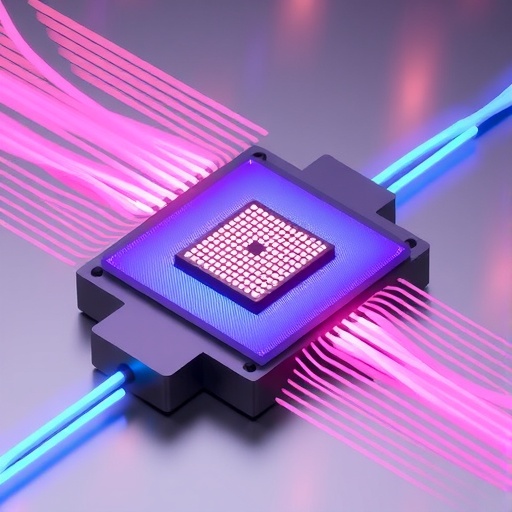
In the ever-evolving landscape of communication and sensing technologies, the underlying components that support these innovations remain critical. Traditionally, complementary metal-oxide-semiconductor (CMOS) devices built on silicon have dominated the semiconductor field. Nonetheless, the exponential increase in demand for higher performance and faster operational speeds introduces formidable challenges. The miniaturization of transistors, a hallmark of the semiconductor industry, is meeting its limits, primarily due to adverse phenomena such as short channel effects and significant contact resistances. In the face of these mounting challenges, researchers are turning their focus toward novel solutions that promise enhanced performance without succumbing to the limitations of conventional technologies.
A recent breakthrough in this pursuit comes from a novel approach to switch design that leverages silicon-on-insulator (SOI) technology in a manner that drastically deviates from traditional fabrication methods. Researchers have demonstrated an innovative system that operates through the manipulation of electric fields and tunneling currents at the juncture between polycrystalline and bulk silicon. This approach offers a paradigm shift for creating high-performance switches, setting the stage for unprecedented capabilities in both power handling and operational speed.
The unique architecture of these switches allows them to achieve a cut-off frequency of 0.75 terahertz, outperforming many existing devices that are confined within the older paradigms of silicon-based transistors. This improvement is crucial because as many electronic systems shift towards millimeter-wave applications, the performance of switches directly affects the speed and reliability of data transmission. With power handling capabilities that are reported to be ten times higher than traditional transistor-based designs, this new switching technology reveals immense potential for applications that require robust performance in high-frequency domains.
What sets these switches apart further is their ability to provide hysteresis-free operation with switching speeds recorded at sub-30 picoseconds. This is an impressive feat, considering that traditional devices often struggle with hysteresis that leads to delays and inefficiencies in signal processing. The ability to switch at such rapid rates not only redefines the boundaries of telecommunications technology but also opens avenues for applications in sensing, where precision and speed are paramount.
Focusing on the broader implications of this research, the new switches have already demonstrated capabilities in millimeter-wave transmitters, achieving data rates that exceed 10 gigabits per second. In today’s data-driven world, where the demand for high-speed data transmission is rapidly increasing, these rates mark a significant advancement. Such a leap forward could facilitate the deployment of next-generation wireless communication technologies, including 6G networks that promise to revolutionize how we connect and interact.
This research reflects a growing trend within the semiconductor industry to rethink the roles of traditional materials and processes. By drawing inspiration from zero-change silicon-on-insulator processes, researchers are unearthing new mechanisms to control and manipulate electronic behavior in ways that were previously overlooked. The ability to harness displacement fields and tunneling currents not only serves as a testament to the ingenuity of modern engineering but also points to exciting new pathways for innovation in electronic devices.
Shifting focus to practical applications, the implications of this technological advancement extend far beyond theoretical interest. The automotive and aerospace industries, for instance, could see transformative changes as high-speed millimeter-wave switches become integrated into systems that require real-time data processing and rapid communications across vast areas. These sectors rely heavily on reliable and high-speed communications, and the advent of these new switches could meet their ever-growing demands for speed and efficiency.
Moreover, the medical field could benefit significantly from this innovation. Applications in imaging, diagnostics, and even telemedicine stand to gain from devices that can facilitate rapid data transfer and processing. High-frequency switches would enable advancements in MRI technology and other diagnostic tools, paving the way for clearer images and more accurate diagnostics that can be transmitted without delay.
Furthermore, the sustainability of semiconductor technology also comes into play as researchers emphasize the potential of this new process to reduce the reliance on complex and cost-intensive fabrication techniques. By using simpler and more versatile processes, manufacturers could lower production costs while also minimizing waste, aligning with global trends toward sustainable technology. This aspect not only appeals to economic considerations but also resonates with growing consumer consciousness around the environmental impact of technology.
In summary, the groundbreaking research on high-power millimeter-wave switches, hinged on displacement fields and tunneling currents, marks a significant milestone in the ongoing quest for faster, more efficient electronic devices. With capacities that transcend current limitations and an emphasis on sustainable practices, this innovation promises to redefine the landscape of communication technology. The evolution from theoretical research into practical applications might just be the game-changer the semiconductor industry has been seeking.
In an age where information travels at lightning speed, and the quest for resonance in data transmission continues unabated, such developments set the stage for a new era of communication technology. As this research gains traction, the entire field of electronics stands to receive the invigorating jolt it desperately needs to propel itself into the future. The implications are profound, and as researchers continue to explore these new frontiers, the possibilities appear limitless. Only time will tell how these high-performance switches will be integrated into everyday technology, but anticipation is undoubtedly building.
Samizadeh Nikoo, M., Eleraky, M., Abdelaziz Abdelmagid, B. et al. High-power millimetre-wave switches on silicon using displacement fields and tunnelling currents.
Nat Electron (2026). https://doi.org/10.1038/s41928-025-01504-0
Cite Scienmag News
Denise Maddox. (January 7, 2026). Silicon-Based Millimeter-Wave Switches Harness Tunneling Currents. Scienmag. https://scienmag.com/silicon-based-millimeter-wave-switches-harness-tunneling-currents/
Denise Maddox. "Silicon-Based Millimeter-Wave Switches Harness Tunneling Currents." Scienmag, 7 January 2026, https://scienmag.com/silicon-based-millimeter-wave-switches-harness-tunneling-currents/. Accessed 4 September 2026.
Denise Maddox. "Silicon-Based Millimeter-Wave Switches Harness Tunneling Currents." Scienmag. January 7, 2026. https://scienmag.com/silicon-based-millimeter-wave-switches-harness-tunneling-currents/


