


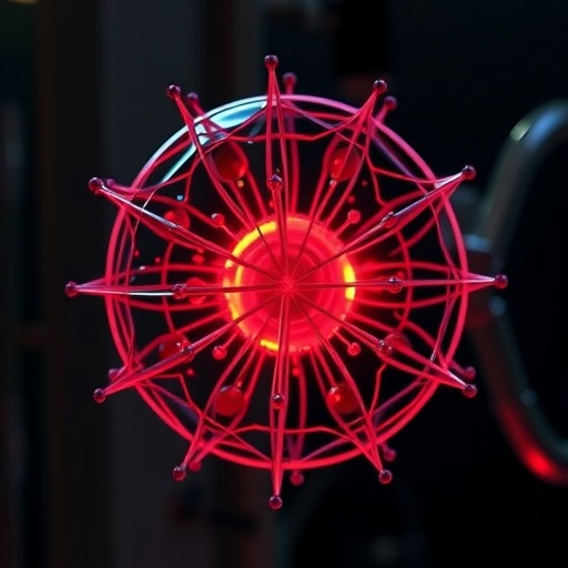
At a time when the United States is racing to rebuild its semiconductor industry, researchers at Kennesaw State University are turning to an unusual classroom tool: interactive visualizations that make the invisible behavior of electrons, photons and other subatomic particles visible to engineering students. The National Science Foundation-funded project is designed to tackle one of electrical engineering’s most persistent challenges—how to help students understand physical processes that occur at scales far below what the human eye can observe. By transforming abstract equations into dynamic simulations, the researchers hope to improve conceptual understanding and encourage more students to pursue careers in the semiconductor sector.
The effort is being led at Kennesaw State by Sandip Das, a professor in the Southern Polytechnic College of Engineering and Engineering Technology; Sheila Hill, a principal lecturer; and Beibei Jiang, an assistant professor. Their work focuses on the university’s required semiconductor devices course for electrical engineering students, where learners study the operating principles of components such as diodes, transistors and other electronic devices. These technologies depend on the controlled movement of charge carriers through solid materials, yet the mechanisms responsible for their behavior unfold at atomic and subatomic scales. That makes them difficult to communicate through conventional lectures, diagrams and textbook explanations alone.
Semiconductors are materials whose ability to conduct electrical current can be precisely controlled. Silicon, the most widely used example, can be modified by introducing carefully selected impurities in a process known as doping. This creates regions with different concentrations of electrons and positively charged “holes,” allowing engineers to construct junctions and devices that regulate current. When voltage is applied, electric fields influence the movement of these charge carriers. At the same time, particles can gain or lose energy, recombine, encounter defects and respond to changes in temperature or material structure. Although students can calculate the expected behavior using mathematical models, they cannot directly watch these events taking place inside a chip.
The Kennesaw State project uses interactive computer animations to bridge that gap. Students first complete learning activities and assessments designed to reveal their initial understanding of semiconductor concepts. They then explore simulations that represent microscopic processes inside semiconductor materials and devices. By changing variables within the modules, students can observe how an altered voltage, material property or device condition affects charge-carrier movement. Follow-up assessments allow researchers to determine whether the visual experience has corrected misconceptions or improved students’ ability to connect equations with physical behavior.
The visualizations were developed by researchers at the Georgia Institute of Technology and are being implemented at five universities, including Kennesaw State. Unlike a static illustration, an interactive simulation can show a system evolving in real time. A student may increase an applied voltage and watch the resulting electric field alter the motion of electrons and holes, or modify a material parameter and observe how the device’s response changes. These interactions are particularly valuable for explaining concepts such as carrier diffusion, drift, energy barriers and recombination—processes that are central to semiconductor operation but often remain hidden behind formal mathematical notation.
“Students often develop misconceptions because we are teaching concepts they cannot physically see,” Das said. “We are talking about electrons, photons, and other quantum particles. Students can read about them in textbooks, but these interactive visualizations help bridge the gap between reading about a concept and truly understanding it.” In semiconductor physics, small misunderstandings can have significant consequences. A student who confuses the direction of electron flow with conventional current, for example, may struggle to explain how a diode functions or why a transistor switches. Visual models give instructors an opportunity to identify these errors and help students revise their mental models.
Kennesaw State faculty are incorporating the modules into lessons and assignments rather than treating them as separate demonstrations. Students can manipulate conditions, make predictions and immediately compare their expectations with the simulated outcome. This process supports active learning, an approach in which students are asked to reason through a mechanism instead of simply memorizing definitions. Purdue University researchers are overseeing the educational assessment, comparing student responses before and after exposure to the visualizations. The goal is to measure whether the tools produce lasting improvements in conceptual learning, not merely short-term gains in test performance.
The project arrives as semiconductor technology becomes increasingly central to economic security, healthcare, transportation and artificial intelligence. Chips control smartphones and computers, power electric vehicles, operate medical equipment and support the data centers behind modern machine-learning systems. The United States is investing heavily in domestic manufacturing, research and workforce development, but expanding production requires engineers who understand both the theoretical foundations and practical behavior of semiconductor devices. “From the moment you wake up until you go to bed, almost everything you do involve semiconductor devices,” Das said. “Whoever has the best semiconductor technology has an advantage across medical, defense, manufacturing and countless other industries.”
The researchers also hope the approach will address a workforce problem that begins before students enter the industry. Many engineering students encounter semiconductor devices as a demanding subject, struggle with invisible and highly abstract concepts, and ultimately decide not to continue in the field. “One of the biggest problems we see is that students get into semiconductors, struggle with the concepts and decide not to pursue the field,” Hill said. “If we can help them understand the material and get excited about it, they can make course choices that prepare them for careers in semiconductor manufacturing, solar power and many other important industries.” Jiang said students are already asking about advanced courses, workshops and career opportunities, suggesting that greater confidence in the classroom may translate into stronger interest in semiconductor careers. Supported by NSF Award No. 2337145, the project could offer a model for making one of modern engineering’s most difficult subjects more visual, intuitive and accessible.
Web References: Kennesaw State University Southern Polytechnic College of Engineering and Engineering Technology; Kennesaw State University Electrical and Computer Engineering
References: U.S. National Science Foundation, Division of Undergraduate Education, Award No. 2337145; semiconductor visualization modules developed by Georgia Institute of Technology; educational assessment led by Purdue University.
Keywords
Semiconductors, electrical engineering, semiconductor education, interactive visualization, engineering education, electrons, charge carriers, silicon, semiconductor devices, workforce development, National Science Foundation, Kennesaw State University
Cite Scienmag News
Katie Riggs. (July 31, 2026). Interactive lessons clarify semiconductor physics for engineering students. Scienmag. https://scienmag.com/interactive-lessons-clarify-semiconductor-physics-for-engineering-students/
Katie Riggs. "Interactive lessons clarify semiconductor physics for engineering students." Scienmag, 31 July 2026, https://scienmag.com/interactive-lessons-clarify-semiconductor-physics-for-engineering-students/. Accessed 5 September 2026.
Katie Riggs. "Interactive lessons clarify semiconductor physics for engineering students." Scienmag. July 31, 2026. https://scienmag.com/interactive-lessons-clarify-semiconductor-physics-for-engineering-students/


