


Copper interconnects are the invisible circulatory system of modern electronics. In every sensor, flexible display driver, and integrated microsystem, microscopic copper lines carry the electrical power and signals that keep devices functioning. Copper remains the metal of choice because it pairs excellent electrical conductivity with relatively low cost, yet producing copper features fine enough for next-generation devices has long demanded a punishing sequence of photolithography, metal deposition, and etching steps. Those processes deliver precision, but they require specialized cleanroom equipment, multiple fabrication stages, physical masks for every design iteration, and they struggle when the target surface is not perfectly flat. Now a research team at Huazhong University of Science and Technology has demonstrated a mask-free alternative that writes dense, highly conductive copper micropatterns directly onto glass, flexible plastic, silicon wafers, and even curved steel, using nothing more exotic than a tailored ink and a femtosecond laser operating in open air.
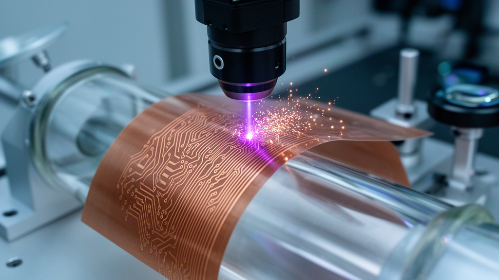
The technique, described in a peer-reviewed publication in the journal Opto-Electronic Manufacturing, is called femtosecond laser direct writing, or FsLDW. The concept is elegantly simple. A copper-containing precursor ink is first coated onto the substrate. A computer-controlled laser beam then scans along a digitally programmed path, converting only the illuminated regions into metallic copper. A rinse removes the unexposed material, leaving behind the desired copper pattern. Because the pattern is defined entirely in software, changing a circuit layout means editing a design file rather than fabricating a new physical mask, a shift that dramatically shortens the path from concept to prototype and makes the method especially attractive for customized and low-volume manufacturing.
Femtosecond lasers are particularly well suited to this kind of precision work. Their pulses last only quadrillionths of a second, concentrating energy inside an extremely small focal region and limiting heat from spreading into the surrounding material. That rapid, localized heating and cooling cycle can promote the decomposition of the precursor, the coalescence of copper particles, and the solidification of a continuous conductor. In principle, this should yield clean, dense copper lines. In practice, earlier demonstrations of laser-induced copper patterning often fell short, producing porous structures with disappointingly high electrical resistance, which undermines the entire point of using copper in the first place.
The Huazhong team, led by Professor Wei Xiong and Associate Professor Hui Gao, identified two main culprits behind those failures. First, residual solvent trapped in the precursor ink could vaporize suddenly under laser irradiation, generating micro-explosions that blasted voids and cracks into the forming metal. Second, uncontrolled copper grain growth during laser exposure prevented the formation of a dense, continuous film. Their solution combined two innovations: a specially formulated particle-free copper precursor ink, engineered to lower the activation barrier for precursor decomposition while keeping grain growth in check, and a pre-drying step that removes the volatile solvent before the laser ever touches the sample. With the explosive ingredient gone and the chemistry tuned, the laser conversion could proceed cleanly.
The results are striking. By systematically optimizing laser power and scanning speed, the researchers produced copper microstructures with line widths below 10 micrometers, roughly a tenth the diameter of a human hair, and a minimum electrical resistivity of 9.34 micro-ohm centimeters, all under ambient conditions without vacuum chambers or inert atmospheres. Low porosity was confirmed across the written lines, and scanning electron microscopy revealed a dense copper surface. The team also showcased two-dimensional copper micropatterns of varying complexity, each generated in a single-step laser writing process, demonstrating that the method is not a laboratory curiosity confined to simple test lines but a versatile patterning platform.
Perhaps the most consequential demonstration is the breadth of compatible substrates. The researchers patterned copper on rigid glass, on flexible polyimide films of the kind used in foldable electronics, across a full two-inch silicon wafer in a wafer-scale process, and on a stainless-steel hemispherical surface, proving that the technique handles curved and nonplanar geometries that defeat conventional lithography. This substrate flexibility matters because the electronics industry is increasingly moving beyond the flat chip. Wearable sensors, conformal antennas, structural health monitors embedded in curved machine parts, and devices built on unconventional surfaces all need conductive interconnects that follow the shape of the object rather than forcing the object to conform to a flat wafer.
To show that the method can build functioning devices rather than just pretty patterns, the team fabricated an ultraviolet photodetector based on tin dioxide, using sequential femtosecond laser writing steps. In that device, the laser-written copper patterns served double duty, acting both as electrodes and as conductive pathways for applying electrical bias and reading out the signal. This device-level demonstration is a critical proof point. It shows that FsLDW can extend beyond material patterning into the fabrication of complete functional microsystems, where interconnects, electrodes, and active elements are produced on the same platform by the same digitally controlled beam.
The practical implications reach well beyond the laboratory. Because copper patterns are defined by programmable laser paths, circuit layouts can be revised as easily as updating a file, collapsing the iteration cycle that traditionally separates a circuit design from a working prototype. The ability to write fine interconnects directly onto substrates of different materials and geometries, including flexible and curved ones, opens the door to copper wiring in places where photolithography is difficult, inefficient, or outright impossible. For applications demanding fine conductive features, rapid design iteration, and direct patterning on flexible, large-area, or curved substrates, the researchers argue that this mask-free approach offers a practical route spanning a wide range of circuit layouts, substrate materials, and surface shapes.
Challenges remain before the technique migrates from laboratory benches to production lines. The team identifies several priorities for future work: increasing processing speed to improve manufacturing throughput, further reducing the resistivity of as-fabricated copper without relying on high-temperature post-treatment, and rigorously evaluating long-term performance under repeated bending, humid environments, thermal cycling, and prolonged electrical operation. Reliability under mechanical stress is the make-or-break question for any flexible electronics technology, since a conductor that works on day one but cracks after a thousand bend cycles is of little use in a wearable device. The researchers also point to multifocal parallel processing and high-speed scanning as routes to boost throughput, and they envision sequentially writing conductive and functional materials so that electrodes, interconnects, and active components all emerge from a single laser-processing platform.
The work emerges from the Micro/Nano Optoelectronics Laboratory at Huazhong University of Science and Technology, an interdisciplinary group recognized as an Innovation Group of Hubei Province that works on laser-based micro and nanomanufacturing, metasurfaces, and holographic display technologies. The broader vision is compelling: a future in which customized electronic systems, from flexible sensors to conformal circuits on curved machine parts, are fabricated as easily as printing a document, with a femtosecond laser tracing dense copper pathways wherever a design demands them. If the remaining hurdles of speed and reliability can be cleared, femtosecond laser direct writing could reshape how engineers think about where, and on what, electronics can live.
Subject of Research: Femtosecond laser direct writing of highly conductive copper micropatterns for flexible and curved electronics
Article Title: Ultrafast lasers enable precise copper circuits on flexible and curved surfaces
Article References: Ultrafast lasers enable precise copper circuits on flexible and curved surfaces. (n.d.). Original publication
Image Credits: AI Generated
DOI: Not provided
Keywords: femtosecond laser, laser direct writing, copper interconnects, flexible electronics, printed electronics, micropatterning, photodetector, mask-free fabrication, conductive inks, curved substrates, micro/nanomanufacturing, Opto-Electronic Manufacturing
Cite Scienmag News
Denise Maddox. (October 17, 2026). Femtosecond lasers print dense copper circuits on flexible and curved surfaces. Scienmag. https://scienmag.com/femtosecond-lasers-print-dense-copper-circuits-on-flexible-and-curved-surfaces/
Denise Maddox. "Femtosecond lasers print dense copper circuits on flexible and curved surfaces." Scienmag, 17 October 2026, https://scienmag.com/femtosecond-lasers-print-dense-copper-circuits-on-flexible-and-curved-surfaces/. Accessed 17 October 2026.
Denise Maddox. "Femtosecond lasers print dense copper circuits on flexible and curved surfaces." Scienmag. October 17, 2026. https://scienmag.com/femtosecond-lasers-print-dense-copper-circuits-on-flexible-and-curved-surfaces/


