


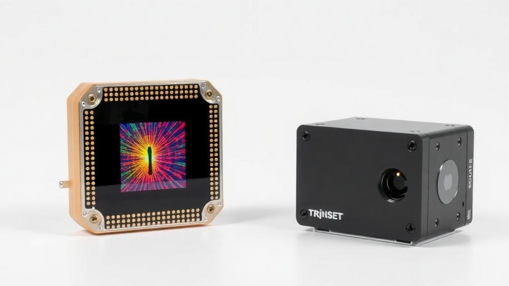
Optical coherence tomography has spent decades as one of medicine’s most trusted imaging tools, peering into the layered structure of the retina and the walls of arteries without cutting a single tissue sample. Now a research team at Shanghai Jiao Tong University has shrunk the technology onto a chip smaller than a grain of rice, and pointed it away from the clinic and toward the factory floor. In a study published in PhotoniX Synergy, the researchers describe a 0.36-square-millimeter photonic integrated circuit that performs swept-source optical coherence tomography, or SS-OCT, with the kind of precision that industrial quality control demands. The system imaged the internal structure of a smartphone camera, measured the thickness of silica wafers with sub-2-micrometer absolute error, and gauged the height of soft photoresist blocks with a relative error below 0.12 percent. A detachable ball-lens fiber probe extends its reach into narrow cavities that conventional microscopes cannot enter.
To understand why this matters, it helps to consider what OCT actually does. The technique works a bit like ultrasound, except it uses near-infrared light instead of sound. A broadband or rapidly swept laser illuminates the sample, and an interferometer compares the weak light reflected from different depths within the sample against a reference path. By analyzing the interference pattern, the system reconstructs a depth profile with micrometer-scale axial resolution. Sweeping the beam across the surface builds up cross-sectional images, and stacking those slices yields full three-dimensional volumes. Because the method is entirely contactless and relies on low-power light rather than ionizing radiation, it can inspect delicate, soft, or transparent materials without deforming or damaging them, a property that becomes invaluable when the object under test is a photoresist layer that a physical probe would smear.
The catch has always been the hardware. A laboratory OCT system typically sprawls across an optical table: a bulky swept laser, discrete fiber couplers, a reference arm with moving parts or modulators, balanced photodetectors, and a maze of alignment-critical connections. That complexity translates into cost, fragility, and maintenance overhead, which explains why OCT has penetrated hospitals far more successfully than production lines. Photonic integrated circuits offer a way out, promising to fold the interferometer, the detectors, and eventually the light source onto chips that can be fabricated by the thousands in semiconductor foundries. But the field has struggled with two persistent problems: choosing a material platform that foundries can manufacture reliably at low optical loss, and designing a flexible sample arm so the chip-bound engine can still reach real-world objects.
The Shanghai Jiao Tong team, led by corresponding author Xingchen Ji, attacked both problems simultaneously. Their chip integrates low-loss silicon nitride interferometers with germanium photodiodes on a commercially fabricated silicon-based platform, combining the distinct strengths of multiple photonic integration technologies in a single device. Silicon nitride is prized in photonics for its extremely low propagation loss and broad spectral transparency, making it ideal for the interferometric heart of an OCT engine. Germanium, meanwhile, absorbs near-infrared light efficiently and serves as the natural photodetector material on silicon. The challenge is that these waveguide platforms have different geometries and optical modes, so the researchers developed an interlayer coupling structure to transfer light between the silicon nitride and silicon layers with a coupling loss of less than 0.15 decibels, a figure low enough to preserve the interference contrast on which OCT sensitivity depends.
The result is a remarkably dense consolidation of optical function. The interferometer and photodetectors occupy a footprint of just 0.9 by 0.4 millimeters, yet the design deliberately keeps the sample arm external, connected through fiber. That architectural choice preserves flexibility: the same chip-based engine can drive different probes depending on the inspection task. Ji emphasized the intent behind the design, saying the aim was to create a compact OCT module adaptable to practical industrial inspections. Integrating the interferometer and photodetectors on-chip reduces the number of discrete optical components, he noted, while the fiber-connected sample arm significantly expands the system’s operational range. In other words, the chip handles the precision optics, and the fiber handles the reach.
Performance figures from the experimental testing suggest the miniaturization did not come at the expense of capability. The system achieved 87 decibels of sensitivity, a measure of its ability to detect weakly reflected light from deep within a sample, along with a 3.42-millimeter sensitivity roll-off range, meaning usable signal persists over a respectable imaging depth. The team resolved internal structures within a smartphone camera module, demonstrating that the chip can inspect the kind of densely packaged, multi-layer consumer electronics that are notoriously difficult to verify non-destructively. Thickness measurements of a silica wafer, compared against established contact-based methods, showed absolute errors below 2 micrometers, while measurements of soft SU-8 photoresist blocks yielded relative errors under 0.12 percent. For semiconductor and microfabrication workflows, where film thicknesses are specified to sub-micrometer tolerances, that level of agreement with reference techniques is the difference between a laboratory curiosity and a production tool.
Perhaps the most striking demonstration involved a probe barely wider than a human hair is thick. By connecting an angle-polished ball-lens fiber probe with a diameter of just 450 micrometers, the researchers captured three-dimensional images of threads hidden inside a metal optical post and of internal layers within a roll of plastic tape. The ball lens focuses the emitted light to a tight spot while the angled polish suppresses back-reflections that would otherwise swamp the weak signal from the sample. This plug-and-play attachment effectively turns the chip-based engine into a miniature endoscope for machines, capable of inspecting bores, threads, and sealed assemblies that no conventional microscope objective can physically access.
Hang Su, the study’s first author and a doctoral student at Shanghai Jiao Tong University, highlighted why contactless operation matters so much in practice. Contactless measurement is invaluable when physical contact could deform a soft surface, Su explained, and the fiber probe allows the team to examine structures that are inaccessible to conventional microscopes. Describing the platform as a plug-and-play OCT module, Su said it paves the way for the next generation of chip-scale OCT engines. That framing captures the broader vision: rather than building a monolithic instrument for one task, the researchers envision a standardized photonic core to which different probes and sample arms can be attached as easily as swapping a lens on a camera.
The commercial implications extend beyond the demonstrations themselves. Because the chip was fabricated on a commercially available silicon photonics platform, the design is compatible with foundry-scale production, which is the prerequisite for driving down OCT system costs to levels that mid-sized manufacturers could justify. The researchers note that complementary technologies, including embedded III-V semiconductor lasers on silicon-on-insulator wafers and chip-based silicon nitride tunable delay lines, could be incorporated to realize a fully integrated, miniaturized OCT system in which even the swept light source lives on the chip. The system described in the paper already integrates a III-V semiconductor light source, silicon nitride interferometers, silicon-germanium photodetectors, and the ball-lens microprobe, drawing on the advantages of each material platform. A Chinese provisional patent application has been filed regarding the technology, signaling the team’s intent to move from demonstration toward deployment.
If that transition succeeds, the implications could reach well beyond metrology labs. Inline, non-destructive inspection of coatings, adhesives, semiconductor packages, medical device surfaces, and additive-manufactured parts could shift from sampling-based quality checks to continuous, three-dimensional verification. The same chip-scale engines could find uses in machine vision systems that need depth information at micrometer resolution, or in compact sensors embedded directly into production equipment. What the Shanghai Jiao Tong team has shown is that the optical complexity that once confined OCT to the optical table can be compressed onto a chip the size of a printed period, without sacrificing the sensitivity or accuracy that made the technique worth shrinking in the first place. The factory floor, long the harder market for optical coherence tomography, may finally be within reach.
Subject of Research: Chip-based photonic integrated circuit for swept-source optical coherence tomography in industrial inspection
Article Title: Compact photonic chip enables three-dimensional OCT inspection for industrial samples
Article References: Compact photonic chip enables three-dimensional OCT inspection for industrial samples. (n.d.). Original publication
Image Credits: AI Generated
DOI: Not provided
Keywords: optical coherence tomography, photonic integrated circuits, silicon photonics, silicon nitride, industrial inspection, non-destructive testing, swept-source laser, ball-lens fiber probe, 3D imaging, metrology, germanium photodiodes, Shanghai Jiao Tong University
Cite Scienmag News
Denise Maddox. (September 30, 2026). Chip-Sized OCT Scanner Brings 3D Industrial Inspection Into Tight Spaces. Scienmag. https://scienmag.com/chip-sized-oct-scanner-brings-3d-industrial-inspection-into-tight-spaces/
Denise Maddox. "Chip-Sized OCT Scanner Brings 3D Industrial Inspection Into Tight Spaces." Scienmag, 30 September 2026, https://scienmag.com/chip-sized-oct-scanner-brings-3d-industrial-inspection-into-tight-spaces/. Accessed 4 October 2026.
Denise Maddox. "Chip-Sized OCT Scanner Brings 3D Industrial Inspection Into Tight Spaces." Scienmag. September 30, 2026. https://scienmag.com/chip-sized-oct-scanner-brings-3d-industrial-inspection-into-tight-spaces/


