In a pioneering leap for nanotechnology and materials science, researchers from the University of Jyväskylä and Aalto University have unveiled a groundbreaking technique that allows for the growth of metal-organic thin films with pinpoint precision, one molecular layer at a time. This innovative approach harnesses laser modification coupled with atomic and molecular layer deposition, enabling the formation of films in highly selective areas on graphene substrates. Such precision not only advances the fundamental science of thin-film fabrication but also opens vast new horizons in the engineering of next-generation photonic and electronic devices.
The cornerstone of this breakthrough lies in atomic layer deposition (ALD), a method historically celebrated in semiconductor manufacturing for its unmatched ability to deposit thin films with atomic-scale control over thickness. Originally pioneered in the 1970s by Finnish physicist Tuomo Suntola, ALD employs sequential, self-limiting chemical reactions that build films layer by layer, ensuring exceptional uniformity and reproducibility. Traditional ALD processes, however, generally produce films over entire substrates, limiting the ability to pattern films with complex shapes or localized functionality without subsequent etching or lithography steps.
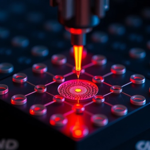
Addressing this limitation, the research team has refined a process known as area-selective atomic/molecular layer deposition (AS-ALD/MLD), wherein thin films grow exclusively on designated regions of the substrate. This control is pivotal for fabricating miniaturized circuits and heterostructures without the destructive and time-consuming patterning steps typical in microfabrication. The technique’s selective nature arises from their ingenious use of laser-patterned graphene, a one-atom-thick carbon lattice renowned for its exceptional electrical, mechanical, and chemical properties.
Graphene’s pristine surface is chemically inert, which ordinarily makes it resistant to film growth through ALD or MLD. By applying focused laser irradiation to graphene sheets deposited on silicon chips, specific surface zones are functionalized with hydroxyl (-OH) groups. These hydroxylated domains serve as nucleation sites where molecular precursors can chemically bond and initiate the growth of europium-organic thin films. This selective chemical activation ensures that subsequent film deposition occurs exclusively in laser-modified regions, leaving unmodified graphene areas untouched, and enabling one-molecule-thick layers to be grown precisely where desired.
The utilization of europium-organic compounds is particularly intriguing due to europium’s photoluminescent properties. When incorporated into thin films, these materials emit light, positioning them as promising candidates for applications in optoelectronics, including light-emitting diodes, displays, and quantum photonic devices. The study presents a model system demonstrating that area-selective MLD can produce complex heterostructures with controlled emission, all facilitated by the underlying laser-patterned graphene template.
Such a methodology leverages the synergy between advanced laser processing and molecular deposition chemistry, pushing the envelope of what is achievable in materials engineering. By enabling spatial control over molecular thin film growth on two-dimensional materials, the method circumvents the need for traditional photolithographic patterning, which often damages delicate layers or introduces defects that degrade device performance. Moreover, the fine-tuning of surface chemistry via laser treatment provides a versatile platform for fabricating a diverse palette of functional materials beyond the demonstrated europium-organic films.
The implications for future technology development are profound. Devices requiring nanoscale precision in structural composition, such as sensors, transistors, and light-harvesting systems, stand to benefit significantly from this approach. The ability to engineer layers with atomic or molecular precision in specifically targeted regions without blanket coating presents a route to integrate multiple functionalities on a single chip, fostering miniaturization and enhanced performance.
Behind this milestone is a collaborative venture combining the University of Jyväskylä’s expertise in graphene laser processing with Aalto University’s pioneering work in molecular layer deposition. This cross-disciplinary synergy exemplifies how merging distinct scientific domains can give rise to unexpected and transformative technological advancements. The researchers express optimism in the potential for industry partnerships to translate these laboratory successes into commercial devices, stimulating innovation across the semiconductor, photonics, and materials sectors.
In reflecting on the journey that led to this achievement, the investigators noted that the initial exploration of graphene surface modification by laser irradiation revealed unexpected capabilities for functionalizing molecular film deposition. This finding was serendipitous, prompting a deeper inquiry into how surface chemistry tailoring could be exploited for selective thin-film growth. Through iterative experimentation and fine control of reaction conditions, the team validated that laser-induced hydroxyl functionalization is sufficiently robust and reproducible for practical manufacturing purposes.
This research, published in the respected journal ACS Nano, presents both the fundamental scientific understanding and demonstration of practical utility. The paper details experimental methods involving graphene substrate preparation, laser patterning protocols, molecular precursor selection, and deposition parameters optimized for area-selective growth. Subsequent characterization using spectroscopic and microscopic techniques confirmed the spatial selectivity and uniformity of the films, alongside their photoluminescent functionality.
The support from the Jane and Aatos Erkko Foundation and the European Research Council’s ERC Advanced Grant project UniEnMLD underscores the strategic importance of advancing atomic and molecular layer deposition techniques. These funding bodies recognize that precision material synthesis at atomic scales is crucial for enabling the next generation of electronic and optical technologies, making this work a vital contribution to the broader scientific enterprise.
As the research progresses toward practical applications, there is an open invitation to industry collaborators to engage with the team. Such partnerships are expected to accelerate the refinement of this methodology and facilitate integration into manufacturing pipelines for electronics, photonics, and sensor platforms. The prospect of custom-designed heterostructures grown directly on patterned graphene substrates presents an alluring future for device engineering, combining scalability with unprecedented material control.
This technological innovation exemplifies the exciting frontier where laser processing meets molecular self-assembly, demonstrating how controlled surface chemistry can dictate the architecture of advanced functional films. By growing europium-organic thin films molecule by molecule on selectively modified graphene regions, the researchers have set a new standard for spatial precision in nanoscale materials engineering, heralding a new era for photoluminescent heterostructures and beyond.
Subject of Research:
Article Title: Area-Selective Atomic/Molecular Layer Deposition of Europium-Organic Thin Films on Graphene and Other 2D Materials for Photoluminescent Heterostructures
News Publication Date: 16-Mar-2026
Web References: http://dx.doi.org/10.1021/acsnano.5c22728
References: ACS Nano journal publication
Image Credits: ACS Nano
Keywords:
Atomic Layer Deposition, Molecular Layer Deposition, Area-Selective Deposition, Graphene, Laser Patterning, Europium-Organic Thin Films, Photoluminescence, 2D Materials, Nanofabrication, Thin Film Growth, Surface Functionalization, Heterostructures
