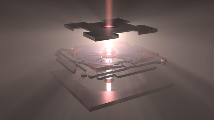
Twisted moiré photonic crystals represent a groundbreaking advancement in the field of optical metamaterials, showcasing immense potential for the miniaturization and enhancement of optical systems. These unique materials are structured in such a way that their layered arrangement allows for the intricate manipulation of light. The principles underlying their operation are akin to the visual phenomena observed when two patterned fabrics are overlapped and slightly misaligned. This misalignment generates new visual patterns, a concept that is harnessed in the functionalities of twisted moiré photonic crystals.
The operational mechanics of these crystals revolve around the interaction between light and the intertwined layers of the material. By adjusting the angle of twist and the inter-layer gap, researchers can fine-tune how the material interacts with different properties of light, such as phase, polarization, and wavelength. Traditionally, measuring all these aspects simultaneously would require multiple optical components. However, twisted moiré photonic crystals promise the potential to consolidate these functions into a singular device, streamlining optical systems.
Despite their promise, the integration of twisted moiré photonic crystals into practical devices capable of real-time manipulation has been a significant challenge. The lack of advanced technologies to control the twist and distance between layers limited their practical applications. Fortunately, a collaborative effort between the Harvard John A. Paulson School of Engineering and Applied Sciences (SEAS), Stanford University, and the University of California – Berkeley has led to the development of an innovative on-chip twisted moiré photonic crystal sensor that utilizes Micro-Electro-Mechanical Systems (MEMS) technology. This advancement has the potential to revolutionize the way photonic materials interact with light.
This newly developed sensor enables real-time control over the twist and distance between crystal layers, allowing it to simultaneously detect and collect comprehensive polarization and wavelength information. The research group’s findings have been published in the esteemed journal ‘Nature Photonics,’ shedding light on how these advancements could reshape various technology sectors, including telecommunications, healthcare, and quantum computing.
The device constructed by the researchers features photonic crystal layers that operate on vertical and rotary actuators, linked to an electrode. Impressively compact, the entire device spans just a few millimeters and can be fabricated through the complementary metal-oxide-semiconductor (CMOS) compatible processes. This compatibility signifies the potential for mass production using existing nanofabrication technologies, paving the way for widespread adoption in numerous applications.
Empirical validation showcased that by manipulating the actuators to alter the distance and rotational alignments of the photonic crystals’ layers, researchers performed simultaneous hyperspectral and hyperpolarimetric imaging. Noteworthy, each pixel captured by the sensor revealed information across the electromagnetic spectrum alongside intricate details regarding the polarization state of the detected light—an unprecedented ability for a device with such active tuning.
The implications of this advanced sensor are vast, extending into several promising applications. For instance, in quantum computing, where precision and information density are paramount, this technology could facilitate breakthroughs in processing capabilities. In medical imaging, enhancing the capacity to discern intricate details about light and color could drastically improve diagnostic outcomes. Furthermore, its utility in satellite communications could lead to advancements in data transfer efficiency via improved imaging techniques.
Looking toward the future, researchers speculate about enhancing these devices with even more sophisticated tuning capabilities. Integrating actuators that provide greater degrees of freedom could further elevate the performance and functionality of twisted moiré photonic crystals, making them more versatile for a range of applications.
The innovative work conducted at Harvard SEAS and its collaborating institutions underscores the transformative potential of twisted moiré photonic crystals in the realm of optical engineering. Eric Mazur, the lead author of the paper, articulates that these materials not only offer tunable optical properties but also resonate with broader application possibilities in advanced photonic technologies. Achieving the precise control demonstrated in this research establishes a scalable avenue toward creating comprehensive flat-optics devices essential for effective light manipulation and information processing.
As this research advances, fostering collaboration between academia and industry will be crucial to transition these laboratory breakthroughs into commercial technologies. The possibilities for practical applications of twisted moiré photonic crystals are extensive and exciting, ranging from enhancing everyday technology to enabling the next generation of devices in various fields.
In conclusion, the realms of optics and photonics stand on the brink of a significant transformation driven by innovation in materials and device fabrication techniques. Twisted moiré photonic crystals may soon pave the way for future technologies capable of reimagining how we manage and harness the power of light across multiple domains.
Subject of Research: Twisted moiré photonic crystals
Article Title: Harnessing Light: The Transformative Potential of Twisted Moiré Photonic Crystals
News Publication Date: N/A
Web References: N/A
References: N/A
Image Credits: Credit: Harvard SEAS
Keywords: Twisted moiré photonic crystals, Optical metamaterials, MEMS technology, Photonic sensors, Light manipulation, Quantum computing, Medical imaging, Photonic devices, Advanced optics, Polarization measurement, Hyperspectral imaging.


