


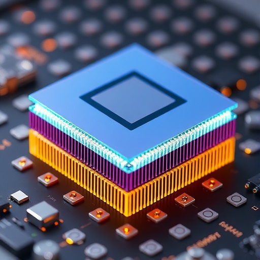
Seoul National University’s College of Engineering has recently made waves in the scientific community by unveiling a groundbreaking roadmap for the engineering of gate stacks, a core technology in the development of two-dimensional (2D) transistors. This innovative research led by Professor Chul-Ho Lee, from the Department of Electrical and Computer Engineering, has significant implications for the future of semiconductor technology. The meticulous work was published in the prestigious journal Nature Electronics, known for its pivotal role in advancing semiconductor technology and achieving high-impact research outputs.
As conventional silicon-based Complementary Metal-Oxide-Semiconductor (CMOS) technology approaches the limits of physical scalability, the semiconductor industry has turned its focus to 2D materials. The physical constraints faced by silicon below the sub-nanometer scale have fueled the need for new materials that can effectively continue to enhance electrical performance while maintaining a small footprint. Emerging 2D semiconductors, characterized by their atomic-level thickness yet stable electrical properties, are being considered as the next evolutionary step in semiconductor technology.
However, despite their promise, these 2D semiconductors face one major impediment to commercialization: the integration of high-quality gate stacks. These gate stacks are critical structures that play a key role in controlling the electrostatic behavior of the transistor channel. As such, the performance and stability of a transistor hinge significantly on the quality of its gate stack. The challenge arises when conventional silicon processes are applied to 2D materials, resulting in degraded quality and an increase in interface defects as well as leakage currents.
In this pivotal study, Professor Lee’s team undertook a comprehensive benchmarking process to compare various gate stack integration approaches. They categorized these methods into five distinct groups, identifying their unique characteristics and evaluating them against critical performance metrics such as interface trap density and equivalent oxide thickness. By benchmarking these technologies, the team established a systematic roadmap that becomes essential for the academia and industry as they strive toward the successful commercial application of 2D transistors.
The research also highlighted innovative approaches, particularly the incorporation of ferroelectric materials within gate stacks. This strategy is poised to revolutionize the field by facilitating ultra-low-power logic applications, non-volatile memory solutions, and enhancing the possibilities for in-memory computing. By detailing the technical prerequisites, including Back-End-of-Line (BEOL) compatibility and low-temperature deposition requirements, the research underscores its real-world applicability and potential in advancing next-generation semiconductor devices.
As the technology landscape evolves toward the post-silicon era, leading semiconductor companies, including major brands like Samsung and Intel, have begun to weave 2D transistor technology into their long-term strategies. The transition from exploring 2D semiconductors as a possibility to actively developing them as a core technology signifies a major leap forward for the industry. Companies have recognized the immense potential that 2D transistors hold for enhancing device functionality, making the need for robust gate stack solutions even more urgent.
The implications of the research extend beyond mere theoretical promise. By providing a well-defined roadmap, the study not only sets clear benchmarks for future research but also enables closer collaboration between academic researchers and industry players. This collaboration is critical for overcoming the remaining barriers to commercialization and driving the development of applications that could impact various fields, including artificial intelligence, ultra-low-power mobile technology, and high-density computing systems.
Professor Lee emphasized the importance of high-quality gate stacks for the successful uptake of 2D transistors in commercial applications. The research team’s findings present a foundational blueprint aimed at addressing the pressing challenges faced by the semiconductor industry. Furthermore, they foresee an expansion of their investigative efforts aimed at the practical integration of these technologies into functional devices.
The lead author of this paper, Dr. Yeon Ho Kim, currently serves as a postdoctoral researcher dedicated to exploring contact and gate stack engineering for 2D transistors. As a foremost contributor to this pivotal research, Dr. Kim is anticipated to play a crucial role in the continued progress of 2D semiconductor technologies, bringing both academic and industrial expertise to the field.
The significance of this research is heightened by its support from pivotal organizations such as the Ministry of Science and ICT in South Korea, which recognizes the potential of next-generation semiconductors. This backing underscores a national commitment to advancing technology that could bolster South Korea’s global competitiveness in the semiconductor landscape.
Furthermore, Seoul National University’s College of Engineering has established itself as a frontrunner in semiconductor research. With a commitment to fostering leaders for the global industry, the College aims to not only advance technological frontiers but also nurture the talent necessary to lead these innovations. The research team, under Professor Lee, continues to be at the forefront of global trends, shaping the course of next-generation semiconductor technologies through their innovative approaches and rigorous scientific inquiry.
In summary, the roadmap for gate stack engineering developed by Professor Lee’s team is expected to pave the way for significant advancements in semiconductor technology. By addressing the key challenges associated with the integration of 2D transistors, this research holds promise for overcoming current limitations and ushering in a new era of high-performance, efficient semiconductor devices that can meet the demands of future computing needs.
Keywords
2D Transistors, Gate Stacks, Semiconductor Technology, CMOS, Ferroelectric Materials, Integrated Devices, Roadmap, Professor Chul-Ho Lee.
Cite Scienmag News
Denise Maddox. (October 14, 2025). SNU Researchers Chart a Path Forward for Next-Generation 2D Semiconductor ‘Gate Stack’ Technology. Scienmag. https://scienmag.com/snu-researchers-chart-a-path-forward-for-next-generation-2d-semiconductor-gate-stack-technology/
Denise Maddox. "SNU Researchers Chart a Path Forward for Next-Generation 2D Semiconductor ‘Gate Stack’ Technology." Scienmag, 14 October 2025, https://scienmag.com/snu-researchers-chart-a-path-forward-for-next-generation-2d-semiconductor-gate-stack-technology/. Accessed 4 September 2026.
Denise Maddox. "SNU Researchers Chart a Path Forward for Next-Generation 2D Semiconductor ‘Gate Stack’ Technology." Scienmag. October 14, 2025. https://scienmag.com/snu-researchers-chart-a-path-forward-for-next-generation-2d-semiconductor-gate-stack-technology/


