


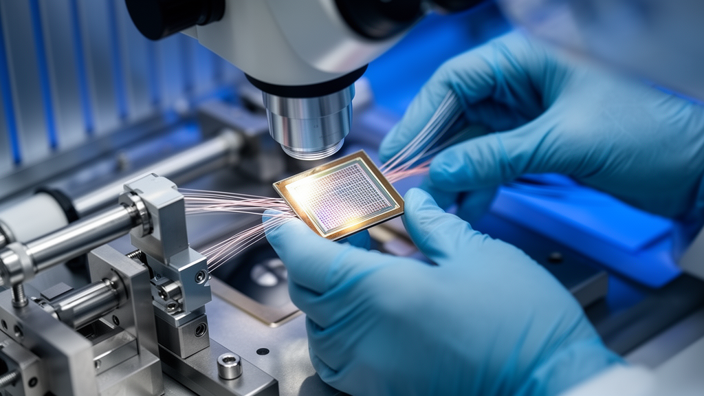
Photonic integrated circuits have spent decades proving themselves in laboratories, carrying light instead of electrons through microscopic waveguides etched onto silicon and silicon nitride chips. They promise faster communications, lower power consumption, and sensors of extraordinary sensitivity. Yet a stubborn obstacle keeps them from following the path that electronic integrated circuits took to global dominance: the packaging problem. A new review published in the journal Opto-Electronic Technology by researchers affiliated with CICECO and the Portuguese photonics company PICadvanced examines why connecting photonic chips to the outside world remains so difficult, and which emerging techniques could finally unlock mass production.
The core challenge lies in the interface between a photonic chip and the optical fibers that carry light to and from it. Unlike electrical contacts, which can tolerate relatively generous alignment errors, optical connections demand near-perfect registration between a fiber core measured in micrometers and an on-chip waveguide of comparable or smaller dimensions. Even a displacement of a few micrometers can produce significant signal loss. The review quantifies this sensitivity with overlap integral calculations showing how insertion loss climbs steeply as a single-mode fiber is displaced laterally from a waveguide, with tolerances on the order of roughly 7 micrometers in one axis and 4.3 micrometers in the other before losses become prohibitive.
Two main families of coupling structures dominate current practice. Grating couplers diffract light vertically between the chip surface and an angled fiber, simplifying testing and packaging but typically suffering from narrow optical bandwidth and the complication of non-normal coupling angles. Edge couplers, by contrast, guide light directly out of the chip facet into a fiber aligned end-on, generally offering lower loss and broader bandwidth but demanding tighter, more expensive alignment. The review systematically compares published coupling approaches across insertion loss, bandwidth, alignment tolerance, fabrication maturity, and relative cost, providing researchers outside the packaging field with a consolidated snapshot of the state of the art.
The performance figures assembled in the review are striking. A two-tier silicon/silicon nitride taper achieved the lowest reported insertion loss of just 0.06 decibels, with a bandwidth of 100 nanometers at less than 0.3 decibels of loss, though alignment tolerance was not reported for that design. Free-form micro-optics created by two-photon polymerization, a technique that uses a focused laser to solidify polymer structures with nanoscale precision, demonstrated 0.5 decibels of insertion loss, a 1-decibel bandwidth of 300 nanometers, and an alignment tolerance of plus or minus 2.2 micrometers. An apodized grating coupler incorporating a metal mirror reached 0.58 decibels of loss with a 38-nanometer bandwidth, while a tapered self-written waveguide approach showed 0.7 decibels of loss with a remarkably forgiving tolerance of plus or minus 5 micrometers.
That last figure may matter more than any raw loss number. Relaxing alignment tolerances is the key that unlocks passive assembly, in which components are placed using mechanical features such as v-grooves and lithographed interconnect structures rather than slow, expensive active alignment loops that search for the optimum position while monitoring the optical signal. Passive assembly allows manufacturers to scale production with current state-of-the-art pick-and-place machinery, transforming packaging from a bespoke craft into an industrial process. For an industry trying to serve telecommunications customers who expect consumer-grade reliability at consumer-grade prices, this shift is arguably the single most important step toward mass production.
Two techniques emerge from the review as particularly promising candidates. Two-photon polymerization has already proven capable of producing devices compliant with Telcordia reliability standards, the qualification benchmarks used in the telecommunications industry, and has demonstrated operation in cryogenic environments, opening the door to quantum applications where photonic chips must interface with superconducting detectors. Self-written waveguides take a different approach: photosensitive materials between the fiber and the chip self-organize into guiding structures when illuminated, effectively letting the optical connection build itself and absorbing alignment errors in the process. Although less mature and more academically rooted, self-written waveguides carry a decisive economic advantage, requiring far less capital investment than two-photon polymerization systems and thereby allowing manufacturers to expand production lines more rapidly.
The review also emphasizes that different industries impose radically different demands on photonic packaging. Telecommunications requires robust, high-performance, cost-efficient devices at consumer volumes. Quantum applications demand exquisite precision and sensitivity, tolerating higher costs in exchange for performance. Biomedical sensing introduces sterilization and biohazard protocols that often dictate single-use sensors, making cost-efficient, high-sensitivity packaging essential for any viable product. The space industry needs devices that combine precision with robustness and radiation resistance. No single packaging approach can serve all of these markets, which is why the authors argue for a consolidated, continuously updated view of the field that helps each sector identify the techniques suited to its constraints.
Automation and intelligence represent the other half of the solution. The review surveys algorithms already being applied to optical alignment, including the classic Nelder-Mead simplex and pattern search methods, alongside more novel approaches such as deep learning, physics-informed neural networks, and artificial intelligence coupled with parallel gradient search. These tools can dramatically shorten the time needed to align fibers to chips, and the authors point toward a broader set of future directions: inverse-designed coupling structures optimized by algorithms rather than intuition, newly engineered materials, wafer-level packaging that processes entire wafers at once, and the use of optical frequency domain reflectometry for precise monitoring during assembly. Together, these advances aim to make packaging more cost-efficient and scalable while preserving the performance metrics each industry requires.
The authors’ vision is unambiguous: photonic integrated circuits will dominate across industries in the twenty-first century just as electronic integrated circuits did in the twentieth, delivering improved performance and efficiency while reducing the cost, size, and weight of optical systems. Whether that vision arrives on schedule depends less on the chips themselves, which are increasingly mature, than on the humble interfaces that connect them to the world. By combining two-photon polymerization, self-written waveguides, nanoimprint lithography, and wafer-level packaging with artificial intelligence, the review argues, the field can dissolve the bottlenecks that currently hold back industries struggling to scale. Increased awareness of packaging as a central engineering discipline, rather than an afterthought, may be what finally carries photonics from the laboratory bench to the consumer’s hands.
Subject of Research: Optical packaging methods and automation for scaling photonic integrated circuits
Article Title: Overcoming packaging challenges could bring photonic chips closer to mass production
Article References: Overcoming packaging challenges could bring photonic chips closer to mass production. (n.d.). Original publication
Image Credits: AI Generated
DOI: Not provided
Keywords: photonic integrated circuits, optical packaging, two-photon polymerization, self-written waveguides, grating couplers, edge couplers, insertion loss, alignment tolerance, wafer-level packaging, artificial intelligence, silicon photonics, mass production
Cite Scienmag News
Denise Maddox. (October 17, 2026). Packaging Bottlenecks Stand Between Photonic Chips and Mass Production. Scienmag. https://scienmag.com/packaging-bottlenecks-stand-between-photonic-chips-and-mass-production/
Denise Maddox. "Packaging Bottlenecks Stand Between Photonic Chips and Mass Production." Scienmag, 17 October 2026, https://scienmag.com/packaging-bottlenecks-stand-between-photonic-chips-and-mass-production/. Accessed 17 October 2026.
Denise Maddox. "Packaging Bottlenecks Stand Between Photonic Chips and Mass Production." Scienmag. October 17, 2026. https://scienmag.com/packaging-bottlenecks-stand-between-photonic-chips-and-mass-production/


