

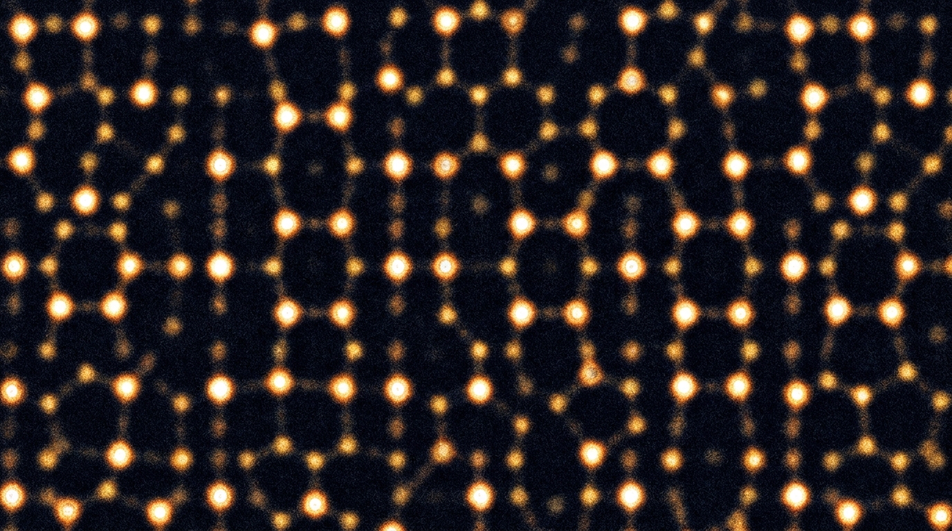
A review published in Applied Microscopy on December 3, 2025, outlines the recent evolution of electron ptychography, a computational imaging technique that utilizes four-dimensional scanning transmission electron microscopy (4D-STEM) to exceed the resolution limits of conventional electron microscopes. The study, authored by Wonwoo Suh, Jeewon B. Choi, Keun-Yeol Park, and Celesta S. Chang, details how quantitative phase retrieval allows researchers to reconstruct the complex transmission function of a specimen, providing both phase and amplitude information. This approach addresses fundamental limitations in traditional microscopy, where intrinsic lens aberrations and the loss of phase information in incoherent detection have historically capped attainable resolution. By leveraging overlapping diffraction patterns from a raster scan, electron ptychography offers a versatile tool for materials characterization, extending from high-resolution imaging of beam-sensitive specimens to three-dimensional reconstruction.
The conceptual foundation of ptychography originated from coherent diffractive imaging, a method where phases are retrieved from continuous diffraction patterns oversampled beyond the Nyquist interval. In 1969, Hoppe and Hegerl extended this concept by proposing that complex wave information could be retrieved from the interference in overlapping regions of diffraction spots. Subsequent formalization by Gerchberg and Saxton in the early 1970s introduced an iterative phase retrieval algorithm that combined interference patterns with a priori known constraints in real space. Fienup later refined these methods by incorporating loosened real-space constraints, improving stability for practical experimental conditions. These algorithmic developments transformed ptychography from a theoretical concept into a robust technique capable of solving for a single, self-consistent transmission function from a set of interdependent diffraction patterns.
Algorithmic approaches in electron ptychography are generally classified into non-iterative and iterative methods. Non-iterative approaches, also known as direct methods, include single sideband (SSB) ptychography and Wigner distribution deconvolution (WDD). SSB ptychography exploits double-overlap regions in reciprocal space to directly reconstruct phase information, offering fast and intuitive reconstruction with good noise tolerance. However, it is primarily suitable for thin, weak phase specimens such as graphene and is difficult to apply to thicker materials where the weak phase approximation no longer holds. WDD applies Wiener filtering in the Wigner distribution domain for deconvolution-based recovery, enabling high-resolution reconstruction but at the cost of high computational intensity and sensitivity to noise.
In contrast, iterative approaches such as the Ptychographic Iterative Engine (PIE), extended PIE (ePIE), Difference Map (DM), and Maximum Likelihood (ML) methods utilize real-space overlaps to impose additional constraints across the dataset. These algorithms update the probe and object functions by utilizing measured intensity data, allowing for the reconstruction of complex structures. The ePIE algorithm, for instance, updates both probe and object functions during the iteration process and has been successfully applied in practical electron ptychography. The ML method reformulates ptychographic reconstruction as an optimization problem in probabilistic terms, providing a powerful way to incorporate experimental uncertainties such as statistical noise. Later developments integrated mixed-state approaches to model partial coherence and other decoherence effects, broadening the technique’s applicability to more complex experimental conditions.
The development of multislice electron ptychography (MEP) has been a significant advancement, enabling the reconstruction of samples with greater thickness and structural complexity. Earlier algorithms relied on the weak-phase approximation, which assumes minimal phase distortion of the electron wave as it passes through the sample. This limitation made atomically thin two-dimensional materials ideal subjects. In 2018, Jiang et al. applied the ePIE algorithm to a twisted bilayer MoS2 with a thickness of 9.8 Å, demonstrating practical feasibility on 2D materials. However, thicker samples presented challenges due to multiple scattering and associated dynamical effects. The multislice method, introduced in 1957, works by dividing the sample into multiple slices and propagating the wavefront sequentially through each slice. Incorporating this approach into ptychographic algorithms allowed for successful reconstruction of thicker specimens, overcoming the limitations of previous methods.
Technological breakthroughs in direct electron detectors have been essential for transforming electron ptychography into a practical imaging technique. The advent of monolithic active pixel sensors (MAPS) and hybrid pixel array detectors (PADs) provided a compelling alternative to traditional charge-coupled device (CCD) cameras, offering improvements in speed, sensitivity, and dynamic range. A primary requirement for these detectors is a wide dynamic range, as ptychographic reconstruction depends on both the intense central beam and weak high-angle scattered signals. Detectors must record variations in electron intensity spanning several orders of magnitude within a single frame without suffering from saturation or underflow artifacts. Most direct detectors adopt either event-based counting or current-based integration strategies to accommodate this broad range of signals, each with distinct advantages and limitations depending on the dose conditions.
Frame rate is another critical factor for effectively recording diffraction patterns for 4D-STEM electron ptychography. To make 4D-STEM acquisition practically comparable to conventional STEM imaging, detectors must operate at hundreds to thousands of frames per second at megapixel resolutions. For example, completing a full 4D-STEM scan recording of 128 by 128 pixel diffraction patterns over a 1024 by 1024 pixel image area within five minutes requires a frame rate of approximately 3.5 kHz or higher. Recent advances in high-speed pixelated detectors now enable frame rates exceeding 1 kHz, allowing data collection at conventional STEM scanning speeds. High frame rates also serve to suppress stage drift and sample vibrations during acquisition, while minimizing radiation damage due to shortened exposure times. The concept of maximum usable imaging speed (MUIS) has been introduced to quantify the trade-off between speed, dynamic range, and noise performance.
Specific detector architectures have been developed to meet these demanding requirements. The EMPAD-G2, developed at Cornell, utilizes a current-integrator-type pixel array architecture with a mixed-mode design combining in-pixel current integration and digital overflow counting. This detector sustains frame rates up to 10 kHz with a near-unity duty cycle, a major improvement over the first generation which was limited to 1.1 kHz. The Arina system, developed by Dectris, utilizes single-electron counting and provides high-speed readout up to 120,000 frames per second. It incorporates Instant Retrigger technology to minimize pulse pile-up, delivering enhanced data quality even under intense electron flux. Timepix3, another event-driven detector, records the arrival time and energy of individual electrons with nanosecond resolution, enabling continuous, shutterless acquisition and dynamic sparse-beam electron ptychography. These detectors have enabled significant progress in achieving wider dynamic range and faster imaging speeds.
Electron ptychography has proven effective in visualizing subtle structural features that are previously inaccessible with conventional microscopy techniques. Due to its significant enhancement in resolution, various features such as single dopants or vacancies can now be resolved. Increasing the tilt angle enhances the visibility of the dopant due to reduced depth blurring, precisely extracting the dopant location along the depth direction. This depth-based analysis can eliminate structural ambiguity in thick samples under strain or bias. Similarly, electron ptychography has been used to resolve distinctive ferroelectric distortions in NaNbO3, capturing structural differences in the bulk region from that of the relaxed surface area. These studies highlight the technique’s capability to resolve subtle localized features at a sub-atomic scale.
The technique is particularly compelling for imaging beam-sensitive materials, which are often damaged under conventional STEM imaging conditions. Electron ptychography reconstructs directly interpretable phase images with inherently higher contrast than Cs-corrected STEM, enabling high-resolution imaging at lower electron doses. The use of a defocused probe in ptychographic acquisition distributes the beam over a larger area, effectively lowering the electron dose imparted to the sample and mitigating radiation damage. Zhang et al. demonstrated ultrahigh spatial resolution imaging of zeolites, successfully resolving individual oxygen atoms in materials that typically tolerate only a few thousand electrons per square angstrom. In chemistry, electron ptychography was used to image beam-sensitive core-shell upconverting nanoparticles, allowing direct observation of structural changes with depth. In biology, low-dose electron ptychography was demonstrated under cryogenic conditions to overcome the low signal-to-noise ratio inherent in cryo-EM, enabling the three-dimensional reconstruction of apoferritin protein at sub-nanometer resolution.
Integrating electron ptychography with conventional tomography enables three-dimensional imaging with high precision. Ptychographic methods provide additional depth sensitivity to overcome limitations in traditional tomography, such as poor contrast for light elements and multiple scattering effects. Ptychographic atomic electron tomography (PAET) has been developed based on tilt series, correcting nonlinear effects arising from multiple scattering and enhancing sensitivity to low-Z elements under significantly reduced electron dose conditions. This approach has been used to determine the structure of complex double-wall carbon nanotube-encapsulated Zr11Te50 structures, observing a new phase that was not previously observed. Additionally, multi-focus electron ptychography has been introduced to enhance depth resolution by acquiring a defocus series within a 4D-STEM framework, offering a more efficient and accessible alternative for three-dimensional analysis without requiring tedious tilting procedures.
Magnetic imaging represents another important application for electron ptychography, where resolving magnetic textures with high spatial resolution has long been a challenge. Imaging non-trivial topological textures from magnetic dipole signals has been achieved using differential phase contrast in Lorentz STEM, but the spatial resolution is fundamentally limited by beam delocalization arising from defocused illumination. By combining a low-noise, high-dynamic-range detector with Lorentz STEM, Chen et al. demonstrated that Lorentz electron ptychography can reconstruct the phase induced by the magnetic flux from skyrmions. Using this method, the internal structure of the skyrmion lattice was visualized through a field direction map with sub-nanometer resolution. This real-space magnetic imaging provides a valuable approach for probing the topology, dynamics, and singularities of spin textures in a range of magnetic materials and spintronic devices.
Despite these recent advances, challenges remain to fully realize the potential of electron ptychography across diverse research fields. The loss of atomic number (Z) contrast poses ambiguity in compositional analysis, as the contrast of reconstructed data does not show a one-to-one correspondence with atomic number but depends on the outer shell valence of each element. While few studies have demonstrated distinguishability between similar-Z elements, achieving a straightforward and broadly applicable Z-sensitivity remains a challenge. Furthermore, while multislice electron ptychography has relaxed the strict thickness limits of traditional reconstruction, successful experimental reconstructions remain challenging in specimens thicker than several tens of nanometers due to multiple scattering and aberration variations. Some recent efforts, such as applying energy filtering to limit inelastic scattering, have shown promise in extending the usable thickness range, but robust and reproducible reconstructions across a broad range of sample thicknesses remain an area of active development.
Looking forward, electron ptychography is expected to evolve beyond static 2D imaging and integrate with emerging STEM experimental schemes. If sufficiently fast acquisition speed and fidelity become available, innovative 4D-STEM acquisition schemes such as in-situ microscopy, tomography, and time-resolved scanning could be combined with electron ptychography. The acquisition of time series 4D-STEM datasets, referred to as 5D-STEM or k-resolved electron correlation microscopy, has been developed to study time-evolving dynamics in nanomaterials. In parallel, time-resolved imaging via multiplexed ptychography has been proposed for optical systems, where diffraction patterns from a series of pulsed illuminations are collected on a direct detector. These emerging experimental modalities suggest that combining ptychography with existing advanced imaging techniques could enable the study of dynamic processes with both structural and phase sensitivity, paving the way for a broader application of electron ptychography in modern STEM workflows across material science, physics, and nanoscience.
Subject of Research: Development of electron ptychography from algorithms, detectors to its applications
Article Title: Development of electron ptychography from algorithms, detectors to its applications
Article References: Suh, W., Choi, J. B., Park, K.-Y., & Chang, C. S. (2025). Development of electron ptychography from algorithms, detectors to its applications. Applied Microscopy, 55(1), Article 13. https://doi.org/10.1186/s42649-025-00119-1
Image Credits: AI Generated
DOI: 10.1186/s42649-025-00119-1
Keywords: Development, electron, ptychography, algorithms, detectors, applications, scientific research
Cite Scienmag News
Denise Maddox. (November 8, 2026). Electron Ptychography Advances Atomic Imaging Resolution. Scienmag. https://scienmag.com/electron-ptychography-advances-atomic-imaging-resolution/
Denise Maddox. "Electron Ptychography Advances Atomic Imaging Resolution." Scienmag, 8 November 2026, https://scienmag.com/electron-ptychography-advances-atomic-imaging-resolution/. Accessed 8 November 2026.
Denise Maddox. "Electron Ptychography Advances Atomic Imaging Resolution." Scienmag. November 8, 2026. https://scienmag.com/electron-ptychography-advances-atomic-imaging-resolution/