
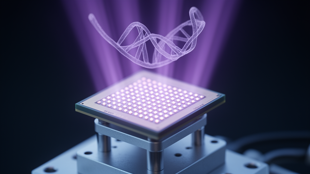
Researchers have built a deep ultraviolet imaging chip from amorphous gallium oxide that can tell apart four fundamental biomolecules in solution without any fluorescent or radioactive labels, and without the bulky spectrometers usually required to do the job. The device, described in AAPPS Bulletin, pairs a light-sensitive gallium oxide film with a commercial amorphous silicon thin-film transistor backplane, the same mass-produced technology that underlies ordinary display screens. The result is a 64 by 64 pixel camera for 254-nanometer ultraviolet light that reads out the characteristic absorption fingerprints of adenine, guanine, L-phenylalanine and L-tyrosine in a single snapshot.
The motivation comes from a persistent bottleneck in biochemical analysis. Quantifying molecules in biological systems is essential for clinical diagnostics, personalized nutrition and food science, yet the authors note that current technologies face fundamental trade-offs between sensitivity, throughput and cost. Conventional methods often rely on complex labeling procedures that add time, expense and chemical complexity. The deep ultraviolet band offers an alternative route, because the purine and pyrimidine bases of nucleic acids and the aromatic amino acids in proteins absorb UV light strongly and in molecule-specific ways. In effect, this spectral region acts as a molecular fingerprint, and a sufficiently sensitive UV photodetector can translate that fingerprint into an electrical signal without any external tag.
Crystalline beta-phase gallium oxide has previously been used to discriminate amino acids thanks to its polarization-dependent photodetection, but integrating that crystalline material with existing read-out electronics is difficult. Its growth requires temperatures above 1800 degrees Celsius and carries high costs. The amorphous form of gallium oxide sidesteps both problems. It can be deposited at low temperature onto a variety of substrates, which makes it compatible with the thin-film transistor technology already deployed at industrial scale. That compatibility is the central design idea of the new work: instead of building a bespoke sensor, the team deposited their functional film directly onto an off-the-shelf backplane.
The fabrication began with radio-frequency magnetron sputtering. A high-purity gallium oxide ceramic target was sputtered in a chamber evacuated to a base pressure of 3.0 times 10 to the minus 4 pascals, with oxygen introduced first to reach 1.6 times 10 to the minus 3 pascals and then argon flowed in at 10 standard cubic centimeters per minute. Working pressure and RF power were held at 0.4 pascals and 60 watts, and a 30-minute deposition produced a film 150 nanometers thick on quartz. For the single-pixel devices, the researchers used standard photolithography and lift-off to pattern interdigital metal-semiconductor-metal electrodes: 75 pairs of transparent indium tin oxide fingers, each 5 micrometers wide with 5-micrometer gaps and 300-micrometer length, defining an effective illumination area of 0.2475 square millimeters.
The electrical performance of the single-pixel detector is the foundation of the sensing scheme. Measured in the dark and under 254-nanometer illumination at 107.17 microwatts per square centimeter across a bias range from minus 10 to plus 10 volts, the device showed an ultra-low dark current of roughly 10 to the minus 13 amperes and a photocurrent of 2.12 times 10 to the minus 7 amperes at 10 volts, a photo-to-dark current ratio of 2.5 times 10 to the sixth. Spectral response measurements from 200 to 600 nanometers revealed a peak responsivity of 0.65 amperes per watt at 255 nanometers with a sharp cutoff at 290 nanometers, a combination the authors say suits the device to anti-interference detection in complex biological backgrounds. Careful control of the oxygen flux during sputtering also suppressed the persistent photoconductivity effect that plagues many oxide photodetectors, yielding a decay time of approximately 50 milliseconds.
Before any biomolecule touched the optical path, the team benchmarked the absorption behavior of the four target molecules with a commercial UV-Vis spectrophotometer. The transmittance spectra established a ranking of ultraviolet absorption capacity: adenine absorbs most strongly, followed by guanine, then L-tyrosine, then L-phenylalanine. Transmittance values extracted at 254 nanometers decayed consistently as molar concentration increased, providing a quantitative reference against which the photodetector results could be judged. The 254-nanometer excitation wavelength was chosen deliberately: compact and inexpensive 254-nanometer sources are readily available, and the wavelength sits almost exactly at the detector’s peak responsivity near 255 nanometers.
The sensing experiment itself was elegantly simple. A cuvette containing biomolecule solution was placed in the optical path between the ultraviolet lamp and the detector, so the liquid acted as a filter attenuating the light before it reached the gallium oxide film. Photocurrents measured for each solution were normalized to a reference value taken with deionized water alone. The normalized photocurrent ratio tracked molar concentration in close agreement with the spectrometer’s transmittance trends. To quantify the agreement, the researchers converted their photocurrents at the minimum tested concentrations into absorbed power ratios using the detector’s nearly linear photocurrent-versus-power relationship, and compared those ratios with the spectrometer’s transmittance percentages at 254 nanometers. The two sets of values were very close, which the authors interpret as evidence that the small solid-state device achieves accuracy comparable to commercial benchtop equipment.
The leap from single pixel to imaging array is where the low-temperature amorphous approach pays off. A 360-nanometer gallium oxide film was sputtered directly onto a commercial amorphous silicon TFT backplane, with the transistors’ exposed drain electrodes serving as bottom contacts and a 40-nanometer indium tin oxide layer added on top. A flexible printed circuit bonded to the substrate connects the array to a compact read-out integrated circuit module and a mobile terminal for real-time display. The geometry matters: under backside illumination, the bottom-gate metal of each transistor shields the amorphous silicon channel from the 254-nanometer light, and the photodetector sits beside the transistor within each pixel, so the imaging signal originates almost entirely from the gallium oxide layer and the ultraviolet exposure does not degrade the backplane. Test images of a hexagonal nut and a hand-written mask came out with well-defined outlines, indicating that crosstalk between pixels is effectively suppressed.
Applied to actual biomolecules, the array produced striking contrast. Four solutions of adenine, guanine, L-tyrosine and L-phenylalanine, all at the same 1 millimolar concentration, were loaded into cylindrical wells in a polydimethylsiloxane container placed in the optical path. The measured photocurrents ranked adenine at 3 times 10 to the minus 10 amperes, guanine at 1.8 times 10 to the minus 9, L-tyrosine at 2.2 times 10 to the minus 9 and L-phenylalanine at 2.5 times 10 to the minus 9, the same absorption ordering obtained from the commercial spectrometer and the single-pixel device. The array also resolved concentration gradients: adenine solutions at 0, 0.1, 0.5 and 1 millimolar produced step-like decreases in photocurrent as concentration rose, with image gray level inversely proportional to concentration.
The authors position the platform as a proof of concept for portable, miniaturized and cost-effective biochemical sensing circuits offering rapid, label-free detection, suited to applications requiring rapid results with moderate precision. Because the amorphous film is deposited at low temperature on mature thin-film transistor technology, the route avoids the integration bottleneck that has limited crystalline ultraviolet detectors, and the researchers argue it opens a path toward mass-producible, large-area biochemical analysis platforms as an alternative to current label-dependent diagnostic methods. As with any demonstration at this stage, the reported results cover four model biomolecules in aqueous solution under controlled laboratory illumination, and translating that performance into real diagnostic workflows will require further validation beyond what this study reports.
Subject of Research: An amorphous gallium oxide deep ultraviolet photodetector and 64×64 imaging array for label-free biomolecule detection
Article Title: Amorphous Ga2O3 deep UV imager for label-free biomolecule detection
Article References: Cai, W., Liang, H., Han, W., Zhu, R., Zhang, Y., Zheng, W., & Mei, Z. (2026). Amorphous Ga2O3 deep UV imager for label-free biomolecule detection. AAPPS Bulletin, 36(1), Article 10. https://doi.org/10.1007/s43673-026-00190-0
Image Credits: AI Generated
DOI: 10.1007/s43673-026-00190-0
Keywords: amorphous gallium oxide, deep ultraviolet, photodetector, label-free detection, biomolecules, thin-film transistor, imaging array, sputtering, UV-Vis spectroscopy, biosensing, adenine, responsivity
Cite Scienmag News
Sylvia Mullen. (October 28, 2026). Amorphous Gallium Oxide Deep-UV Imaging Array Detects Biomolecules Without Labels. Scienmag. https://scienmag.com/amorphous-gallium-oxide-deep-uv-imaging-array-detects-biomolecules-without-labels/
Sylvia Mullen. "Amorphous Gallium Oxide Deep-UV Imaging Array Detects Biomolecules Without Labels." Scienmag, 28 October 2026, https://scienmag.com/amorphous-gallium-oxide-deep-uv-imaging-array-detects-biomolecules-without-labels/. Accessed 29 October 2026.
Sylvia Mullen. "Amorphous Gallium Oxide Deep-UV Imaging Array Detects Biomolecules Without Labels." Scienmag. October 28, 2026. https://scienmag.com/amorphous-gallium-oxide-deep-uv-imaging-array-detects-biomolecules-without-labels/