The field of nanoimprinting lithography (NIL) has seen substantial advancements over the past three decades, and the innovation continues to gain momentum across various industries. A pivotal review encapsulating this evolution, authored by Professor L. Jay Guo’s research team at the University of Michigan, details the critical milestones and future trajectories of NIL in the inaugural issue of the journal Opto-Electronic Technology. This comprehensive overview serves not only as a retrospective but also as a roadmap for the ongoing advancement of nanomanufacturing processes.
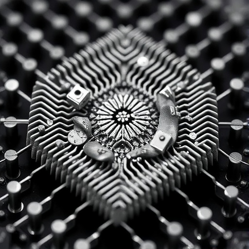
Nanoimprinting lithography is a highly precise technique for patterning nanoscale features on substrates, utilizing molds to create intricate designs that are vital for diverse applications. The review delves deep into the two predominant methods of NIL—thermal NIL (T-NIL) and UV NIL (UV-NIL)—offering an exhaustive analysis of the various molds, photoresists, and imprinting techniques associated with each method. The discussion extends to the distinctive characteristics, strengths, and shortcomings of each approach, providing a nuanced understanding of their operational dynamics.
Thermal NIL, pioneered by researchers like Chou, utilizes heat to facilitate the imprinting process. While it offers high resolution and fidelity, the challenges of temperature management and mold durability pose considerable hurdles. In contrast, UV NIL relies on photopolymerization to achieve rapid curing of photoresists, thereby allowing for more flexible processing conditions. However, issues related to the uniformity of exposure and pigment conversion remain key concerns to be addressed. The research team meticulously evaluates methods such as plate-to-plate NIL, step-and-repeat NIL, and roller-based NIL, highlighting their applicability in real-world manufacturing scenarios while noting the inherent challenges each method encounters.
The review draws attention to significant breakthroughs in NIL technology, emphasizing its crucial role in semiconductor manufacturing, flat optics, and biomedical applications. Canon’s innovation—the FPA-1200NZ2C—marks a monumental achievement as the first semiconductor-grade NIL equipment tailored for high-resolution applications. This device epitomizes the journey toward achieving minimal defect rates and exceptional throughput while maintaining industry standards. Furthermore, the application of NIL techniques in developing meta-lenses has transformed conventional optics, integrating advanced functionalities in smartphones, automotive lidar systems, and augmented reality devices.
On the academic front, the research landscape surrounding NIL is diversifying with increasing complexity and scope. Researchers are focusing on high-quality optical device fabrication, investigating the precise control of molecular orientation in semi-crystalline polymers, and examining strain engineering for property optimization. Furthermore, inventive techniques such as polymer fiber imprinting, laser-assisted imprinting, ultrasonic NIL, and electrochemical imprinting are emerging, opening new avenues for exploration and application. These advancements underscore NIL’s versatile applicability beyond traditional domains, highlighting its potential to revolutionize electronics, biosensors, flexible electronics, and wearables.
Despite the significant progress achieved, challenges remain formidable. Managing defect density, controlling residual layer thickness, and ensuring precision alignment continue to be pressing issues in the realm of NIL. However, ongoing research efforts and interdisciplinary collaborations promise to pave the way for innovations that may overcome these obstacles. As industries increasingly seek solutions to meet the growing demand for nanomanufacturing capabilities, the industrialization of NIL appears to be on the horizon, potentially ushering in a new era characterized by high-precision manufacturing techniques.
The significance of this review goes beyond the specifics of NIL; it encapsulates a broader narrative of technological progression and industrial applicability. Through systematic examination of methods and applications, Professor Guo’s research group captures the essence of an evolving field that is ripe for exploration and enhances the understanding of NIL’s role in the current technological landscape.
Professor L. Jay Guo’s stature shines brightly in the realm of electrical engineering and computer science. As the Emmett Leith Collegiate Professor at the University of Michigan and a distinguished fellow of both IEEE and Optica, his expertise lends considerable weight to the review. His team’s focus on high-resolution lithography and nanoimprinting processes significantly contributes to advancing technologies in photonic sensors, photovoltaic detectors, and flexible transparent conductors. With over 295 peer-reviewed publications and more than 35,000 citations to their credit, the team’s impact resonates throughout the scientific community.
The thorough synthesis of thirty years of nanoimprint research encapsulated in this review serves as a compelling reference for industry leaders, researchers, and future innovators. It underscores the transformative potential of NIL in various sectors and emphasizes the necessity for continued research and development efforts to unlock the full capabilities of this groundbreaking technology.
As we witness the ramifications of these advancements on the global stage, the imperative for cross-disciplinary approaches to problem-solving becomes increasingly clear. By fostering collaborations that bridge the gap between industry and academia, researchers can drive innovation further, establishing NIL as a cornerstone of modern manufacturing processes. In this light, the future of nanoimprinting lithography is not just a tale of technical achievements; it represents a paradigm shift in how we conceive and create with nanoscale materials.
Through pathways illuminated by rigorous research and practical application, the field of nanoimprinting is set to flourish across a plethora of domains. The collective effort of researchers worldwide will undoubtedly elevate NIL to new heights, fundamentally reshaping industries and enabling the next generation of cutting-edge technologies. The journey has just begun, and its implications will resonate for years to come.
As we look toward the future, the collaborative spirit and relentless pursuit of knowledge in nanoimprinting lithography signify that substantial contributions to human ingenuity and technological development lie ahead. The concerted efforts of Professor Guo and his research group herald an era where nanomanufacturing not only meets the challenges of today but also anticipates the needs of tomorrow, ensuring that the legacy of innovation continues unabated.
The review encapsulates more than just a technical analysis; it is a clarion call for recognizing the integral role of nanoimprinting lithography in our ever-evolving technological sphere. With an understanding of the underlying methods, challenges, and breakthroughs highlighted within this review, we are better equipped to navigate the future landscape of nanomanufacturing and embrace the uncharted possibilities that lie ahead.
Subject of Research: Nanoimprinting Lithography
Article Title: OET Inaugural Cover | 30 Years of Nanoimprint Lithography: Leading the New Era of Nanomanufacturing
News Publication Date: 17-Jul-2025
Web References: Opto-Electronic Technology
References: DOI: 10.29026/oet.2025.250001
Image Credits: Wei-Kuan Lin, L. Jay Guo
Keywords
Nanoimprinting, Lithography, Nanomanufacturing, Semiconductor, Photonics, Optical Devices, Nanoscale, High Resolution, Manufacturing Processes.
