

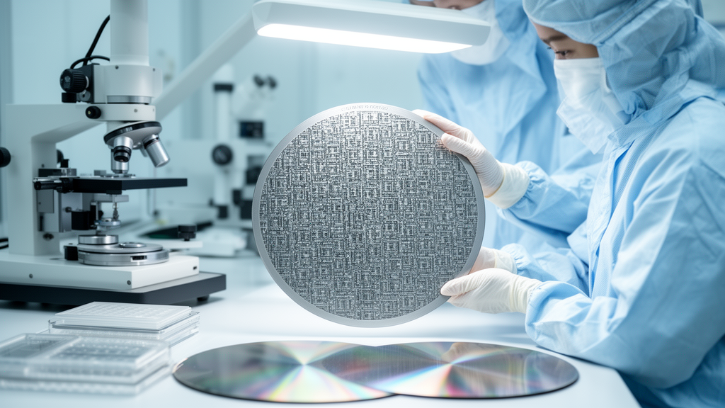
Researchers at Kyoto University have demonstrated that a silicon carbide transistor structure capable of operating at 600°C can be fabricated on a 6-inch epitaxial wafer, advancing the technology from chip-scale experiments toward integrated-circuit production. The experimental device was a junction field-effect transistor, or JFET, made using an ion-implantation-based side-gate process. In the first wafer-scale fabrication trial, threshold voltages within the wafer’s center region showed high uniformity, with a standard deviation of less than 0.07 volts. The result indicates that a process previously developed in a university laboratory can be transferred to an industrial fabrication environment without major obstacles, while also revealing that wafer-level uniformity exceeded the researchers’ expectations.
The achievement addresses one of the central manufacturing challenges facing high-temperature silicon carbide electronics: producing many small, consistent devices on a single wafer. The university team adapted much of the JFET fabrication process used in its earlier chip-scale work to wafer scale, taking account of manufacturability at industrial standards. To overcome the equipment limitations of a university laboratory, the researchers collaborated with Phenitec Semiconductor Corp., which operates a mass-production fabrication plant. The resulting transistor was fabricated on a 6-inch SiC epitaxial wafer, and the successful process transfer provides an experimental basis for developing integrated circuits based on the device structure.
Kyoto University described the result as a technical milestone because integrated circuits require large numbers of compact, electrically similar transistors rather than a single laboratory component. The reported threshold-voltage measurement provides evidence of within-wafer consistency, but the release does not characterize the full electrical performance, yield, reliability or long-term behavior of devices across the entire wafer. It also does not establish that complete integrated circuits or practical commercial products have already been produced. Instead, the study shows that the established JFET fabrication sequence can be implemented at wafer scale and that the first trial produced uniform devices in the wafer center, an outcome the research team said was better than anticipated.
The devices build on the team’s previous work on a silicon carbide transistor that operates at 600°C. That temperature tolerance is the defining performance claim relevant to electronics intended for extreme environments, although the present announcement focuses on scaling the fabrication process rather than introducing a new operating-temperature record. The combination of the earlier high-temperature device research and the current wafer-scale demonstration broadens the reported manufacturing path toward silicon carbide integrated circuits. Potential application areas identified by the research team include jet-engine sensors, geothermal-resource development and exploration of Venus, but the release presents these as prospective areas rather than demonstrated uses of the fabricated transistors.
First author Mitsuaki Kaneko said the researchers had expected wafer-scale device fabrication itself to succeed but were surprised by the degree of uniformity in the center region during the first fabrication trial. He also emphasized the distance between creating a device in a laboratory and deploying it in society. The Kyoto University–Phenitec collaboration was intended to help close that gap, and the researchers are aiming to establish a startup, although they acknowledge that substantial challenges remain. The immediate scientific achievement is therefore not a finished silicon carbide circuit or a ready-made extreme-environment sensor; it is the successful transfer of a previously laboratory-scale JFET process to a 6-inch wafer, accompanied by a measured demonstration of threshold-voltage uniformity and a step toward evaluating the technology at production-relevant scale.
Subject of Research: Experimental wafer-scale fabrication of 600°C silicon carbide junction field-effect transistors for extreme-environment integrated circuits.
Article Title: Lab to fab at the wafer-scale for SiC
Article References: Lab to fab at the wafer-scale for SiC. Original publication (Bibliographic details unavailable.)
Image Credits: AI Generated
DOI: Not provided
Keywords: silicon carbide, JFETs, wafer-scale fabrication, high-temperature electronics, integrated circuits, threshold-voltage uniformity, ion implantation, Kyoto University, Phenitec Semiconductor, semiconductor manufacturing, wafer-scale, scientific research
Cite Scienmag News
Denise Maddox. (October 22, 2026). Researchers scale heat-resistant silicon carbide transistors to 6-inch wafers. Scienmag. https://scienmag.com/researchers-scale-heat-resistant-silicon-carbide-transistors-to-6-inch-wafers/
Denise Maddox. "Researchers scale heat-resistant silicon carbide transistors to 6-inch wafers." Scienmag, 22 October 2026, https://scienmag.com/researchers-scale-heat-resistant-silicon-carbide-transistors-to-6-inch-wafers/. Accessed 22 October 2026.
Denise Maddox. "Researchers scale heat-resistant silicon carbide transistors to 6-inch wafers." Scienmag. October 22, 2026. https://scienmag.com/researchers-scale-heat-resistant-silicon-carbide-transistors-to-6-inch-wafers/