The efficient transport of charge carriers is a cornerstone requirement for the advancement of high-performance light-conversion devices, particularly in the rapidly evolving fields of optoelectronics and renewable energy technologies. Two-dimensional (2D) perovskites, while promising materials for such applications, encounter substantial challenges attributable to their unique quantum well (QW) structures. In these materials, the inorganic layers are confined by organic cation spacers, leading to pronounced exciton binding energies. This phenomenon hampers the dissociation of excitons into free carriers, significantly impacting carrier transport properties and ultimately constraining the efficiency of devices built upon these materials.
Understanding the underlying physics of electron-hole behavior in 2D perovskites has been a formidable task for researchers. One of the primary hurdles stems from the substantial influence exerted by surface states, a factor that is challenging to investigate through conventional methods. The lack of advanced real-time, surface-sensitive characterization techniques has rendered it difficult to elucidate how surface phenomena govern carrier dynamics in these materials. As such, there has been a pressing need to develop innovative tools that can provide insights into these critical processes at an unprecedented temporal and spatial resolution.
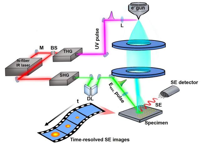
Addressing this void in knowledge, a team of scientists spearheaded by Professor Omar F. Mohammed at King Abdullah University of Science and Technology (KAUST) has published groundbreaking findings in the journal Light: Science & Applications. They employed an advanced technique known as scanning ultrafast electron microscopy (SUEM), which offers an extraordinary capacity for mapping surface charge carrier diffusion with unmatched surface sensitivity. This method enables researchers to visualize the behavior of photo-generated carriers in real time, a capability that allows for a deeper understanding of how these carriers move across the surface of 2D perovskite materials after being excited by photons.
The research undertaken by Mohammed and his colleagues revealed astonishing photo-induced surface carrier diffusion rates. Their measurements indicated values of approximately 30 cm²/s for n=1, 180 cm²/s for n=2, and a remarkable 470 cm²/s for n=3. These figures are startling as they surpass bulk carrier diffusion rates by over twentyfold. To substantiate their findings, the team conducted Density Functional Theory (DFT) calculations, which confirmed that the enhanced diffusion rates observed at the surface can be attributed to broader charge carrier transmission channels in the surface region compared to those found in the bulk material. Such insights are crucial for optimizing the design and functionality of devices that utilize 2D perovskite materials.
In discussing the implications of their research, the team expressed the significance of their ability to directly image the transport of photo-generated charge carriers at ultrafast timescales using SUEM. They emphasized the unique surface-sensitive capability of this technique, which allows for unprecedented exploration into carrier diffusion in localized regions immediately following photoexcitation. This depth of analysis presents a clear distinction from traditional bulk or ensemble spectroscopic techniques, which often fail to accurately differentiate between surface and bulk states, particularly in complex materials like 2D perovskites.
The findings from this research not only illuminate the distinct differences between surface and bulk transport mechanisms but also open up new avenues for enhancing the performance of 2D perovskite-based optoelectronic devices. Such advancements could facilitate the development of highly efficient solar cells, photodetectors, and light-emitting devices, thereby pushing the boundaries of what is possible in the realm of light conversion technologies.
The work conducted by Mohammed and his team represents a significant step forward in the quest to optimize 2D perovskite materials for practical applications. The ability to visualize and understand carrier dynamics directly at the surface level allows scientists and engineers to devise sophisticated strategies for interface engineering, ultimately leading to improved device architectures. This breakthrough signifies a turning point for research in this area, as it enables the tailoring of material architectures in a manner that enhances charge carrier mobility and boosts overall device efficiency.
Moreover, these results might inspire future investigations into other materials exhibiting similar quantum confinement effects. The principles uncovered in this study could very well be applicable to a wide range of materials beyond just 2D perovskites, indicating a broader impact on the field of optoelectronics. By bridging the gap between theoretical modeling and practical observation, researchers can accelerate the pace of innovation and enhance our understanding of electronic properties in novel materials.
As the researchers continue to explore the implications of their findings, there is a growing anticipation for future work that leverages SUEM to investigate the carrier dynamics in other promising materials. The combination of ultrafast temporal resolution and surface sensitivity positions SUEM as an indispensable tool in the materials science toolkit, one that holds the potential for various applications across different domains, from energy harvesting to advanced electronics.
In summary, the research led by Professor Omar F. Mohammed has unveiled crucial insights into the behavior of photo-generated surface carriers in 2D perovskites, revealing significant differences between surface and bulk transport properties. Such findings not only deepen our understanding of these advanced materials but also set the stage for future developments that could revolutionize the field of optoelectronics.
Subject of Research: Surface charge carrier transport in 2D perovskites
Article Title: Real-space imaging of photo-generated surface carrier transport in 2D perovskites
News Publication Date: [Not provided]
Web References: [Not provided]
References: DOI 10.1038/s41377-025-01758-5
Image Credits: Credit by Lijie Wang, Wentao Wu et al.
Keywords: 2D perovskites, charge carriers, ultrafast electron microscopy, surface transport, exciton binding energy, optoelectronics, Density Functional Theory, carrier diffusion.
