

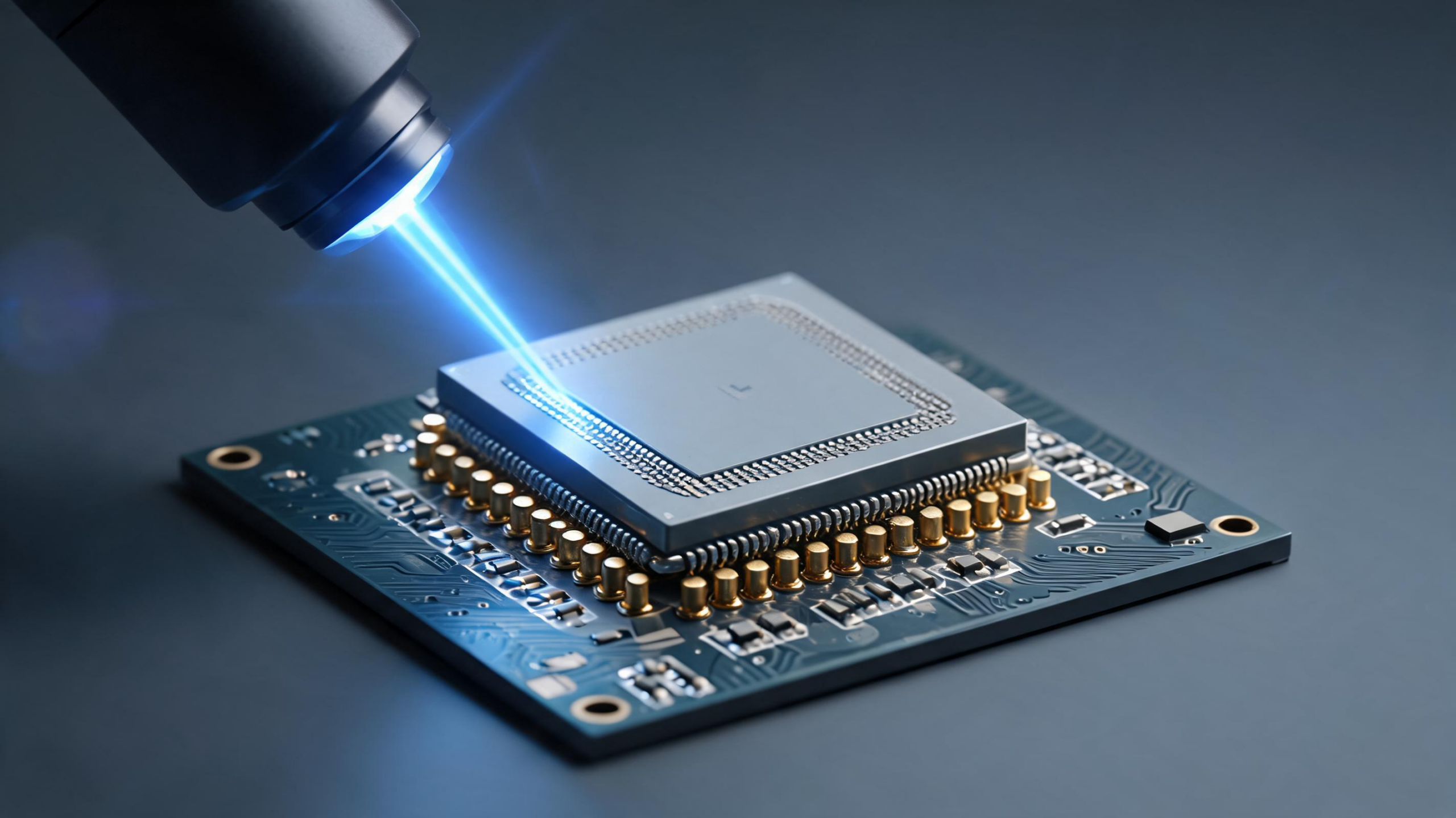
A burst of femtosecond laser pulses has been used to selectively thin gold plating on electronic bonding pads, addressing a long-standing conflict in advanced packaging. Gold protects contacts and supports reliable wire bonding, but when too much dissolves into molten solder it can generate brittle gold–tin intermetallic compounds that weaken connections. In a study published in Advanced Materials Joining, researchers used localized laser processing to reduce a gold layer from about 3.0 micrometers to approximately 0.3 micrometers. The treated pads produced solder joints that spread more evenly, developed far less interfacial reaction product during accelerated aging, and retained substantially greater mechanical strength than untreated thick-gold pads. The approach is aimed at substrates that must combine different functions in neighboring regions: thick gold where wire bonding or wear resistance is required, and thin gold where soldering performance is more important. Rather than replacing established surface finishes across an entire component, the researchers describe femtosecond processing as a post-plating method for creating this local distinction.
Gold plating is widely used in electronics because it resists corrosion and provides a dependable surface for electrical contact and bonding. Its thickness, however, must be matched to the job. High-reliability wire-bonding regions may need a relatively thick coating for structural stability and resistance to wear, while surface-mount or flip-chip soldering pads generally perform better with a much thinner gold layer. During reflow, the molten solder reacts rapidly with gold. Excess dissolved gold can combine with tin to form gold–tin intermetallic compounds, or IMCs, whose hardness and brittleness make them vulnerable to cracking. As the joint ages, these compounds can thicken, consume tin from the solder, encourage lead-rich segregation in tin–lead systems, and create stress concentrations. Conventional solutions include designing different plating regions during fabrication, using specialized finishes such as electroless nickel electroless palladium immersion gold, or removing gold through tinning. Those choices can add process complexity or may not offer the precise, non-contact, pad-level control needed for mixed-function substrates.
The researchers fabricated test samples with an aluminum oxide substrate and an Au/Ni/TiW multilayer structure. The nickel layer was 4 micrometers thick and the TiW layer was 10 micrometers thick. They prepared gold coatings of different starting thicknesses for laser optimization and joint testing, then scanned selected surfaces with a femtosecond laser operating at a central wavelength of 1030 nanometers and a repetition rate of 1 megahertz. Femtosecond pulses deliver energy over extremely short intervals, allowing material removal through high peak power and nonlinear optical effects while limiting the time available for heat to diffuse into surrounding material. The team varied energy density, scanning speed, scan spacing, and the number of passes, measuring both the depth removed and the resulting surface roughness. Under optimized conditions, a 3-micrometer coating was reduced to about 0.3 micrometers, within the 0.13-to-0.45-micrometer range identified in the study for surface-mount pads.
The laser did more than reduce the amount of gold. It also transformed the surface into a field of directional micro-grooves and ripples. Increasing the energy density increased the thinning depth, but excessive energy produced bulges, burrs, and spatters. Faster scanning reduced the overlap between adjacent laser spots and generally decreased the removal depth, while repeated passes continued to remove material with diminishing returns. Increasing the scan pitch produced sparser, more step-like features and reduced the depth of thinning. These relationships gave the researchers a way to balance material removal against surface quality. The resulting texture influenced the way molten solder moved across the pad. In terms of wetting, the roughened surface increases the actual contact area, and the grooves can provide capillary pathways that help draw liquid solder across the interface. The effect is consistent with the Wenzel model, which relates apparent contact angle to the ratio between rough and smooth surface areas, although the investigators distinguish the texturing effect from the chemical effect of reducing the gold inventory.
That distinction was important in the soldering experiments. The team used 63Sn37Pb solder balls with a diameter of 500 micrometers and compared untreated thick-gold pads with laser-treated pads. At temperatures from 205 to 250 degrees Celsius, solder on the treated surfaces achieved spreading coefficients between 95.35% and 97.20% after 90 seconds. Untreated surfaces showed lower and more temperature-sensitive values, ranging from 77.45% at 205 degrees to 93.11% at 250 degrees. The treated solder spread in an elliptical, directionally influenced shape that reflected the laser grooves, whereas solder on untreated pads was more nearly circular and could form a basin-like profile with raised edges. On the thick-gold surfaces, rapid gold dissolution created stronger composition gradients and promoted material redistribution toward the perimeter. By reducing the gold available for that reaction and adding pathways for capillary flow, the processed pads reached stable spreading more quickly and produced more uniform joint shapes. The results indicated that an isothermal dwell of at least 30 seconds was sufficient for wetting under the reported conditions.
Microscopic analysis showed how the altered gold thickness affected the joint during reflow and subsequent aging. Gold dissolved from both treated and untreated surfaces during soldering, and both produced gold–tin or gold–nickel–tin compounds in the solder matrix. The principal interfacial layer was nickel-rich Ni3Sn4. Yet the treated joints contained finer, needle-like intermetallic features measuring about 10 to 15 micrometers, compared with coarser, lath-shaped compounds larger than 25 micrometers in the untreated joints. The researchers then aged the samples at 150 degrees Celsius for as long as 500 hours to accelerate diffusion and interfacial reactions. After that period, the total IMC thickness in untreated joints had grown from 1.254 to 36.753 micrometers. In laser-treated joints, it increased from 1.188 to 8.121 micrometers, representing a reduction of more than 75% relative to the thick-gold comparison. The smaller residual gold inventory limited the amount of material available for gold–tin compound formation and redeposition, which was identified as the main reason for the suppressed growth.
The aging process also revealed differences in chemical segregation and damage development. In untreated joints, pronounced lead-rich phases appeared above the gold-containing intermetallic layer, becoming continuous by 250 hours and exceeding 10 micrometers after 500 hours. Such brittle regions can provide preferred routes for crack propagation. Laser-treated joints suppressed the formation of a continuous lead-rich layer, consistent with lower tin consumption by gold. The experiments also tracked voids, which can reduce thermal conductivity and mechanical integrity. After 500 hours, untreated joints reached a void ratio of 9.23%, while the laser-treated joints remained below 1.0%, with a measured value of 0.32%. The researchers link this difference to reduced growth of thick gold-containing IMCs and lower accumulated interfacial stress, while the improved spreading and more uniform contact may also have reduced localized reaction conditions that favor void development. These results suggest that controlling the surface before soldering can influence several later stages of joint degradation rather than only the initial wetting event.
Mechanical tests provided a direct measure of the reliability difference. Shear testing was performed at a height of 200 micrometers and a speed of 200 micrometers per second. Before aging, laser-treated joints carried 44.6 newtons, compared with 40.9 newtons for untreated joints. After 500 hours at 150 degrees Celsius, the treated joints retained a shear load of 28.4 newtons, or 63.68% of their initial value. Untreated joints fell to 13.3 newtons, retaining only 32.52%. The treated joints therefore carried more than twice the load of the untreated joints after aging. Fracture surfaces offered a structural explanation: aged thick-gold joints displayed smooth regions and exposed nickel pads, characteristic of brittle failure along the interfacial reaction layer. Treated joints showed scratch marks and dimpled rupture surfaces dominated by tin and lead, indicating that fracture remained within the more ductile solder. The authors note that treated-joint strength increased slightly during the first 50 hours, from 44.6 to 46.6 newtons, possibly because controlled growth of Ni3Sn4 initially reinforced the interface without producing excessive brittle gold–tin compounds.
The findings position femtosecond laser thinning as a complementary manufacturing strategy rather than a universal replacement for selective plating, ENEPIG, or conventional gold-removal methods. Its principal advantage is localized, post-plating control: selected soldering pads can be converted from thick gold to a thin, solder-compatible surface while adjacent wire-bonding or contact areas remain unchanged. Under the reported settings, the nominal scan area rate was approximately 1.7 square millimeters per second, and a 2-by-2-millimeter pad required about 2.35 seconds of calculated laser exposure, excluding positioning, focusing, and handling. The study used 63Sn37Pb solder partly because its interfacial reactions make gold dissolution, redeposition, lead-rich-layer formation, and aging effects readily measurable, and partly because tin–lead solder remains relevant to some high-reliability applications. The authors caution that the method’s performance with lead-free alloys such as Sn–Ag–Cu still requires further study. Even with that limitation, the work demonstrates a precise physical route for tailoring a critical interface, potentially helping manufacturers reconcile the opposing demands of robust bonding contacts and durable, soldered microelectronic connections.
Subject of Research: Femtosecond-laser thinning of gold pads for reliable flip-chip solder bonding
Article Title: Femtosecond laser-based surface gold removal and its applications in flip chip bonding
Article References: Qu, Z., Kong, W., Li, Y., Peng, Y., Wang, D., Wang, K., & Li, X. (2026). Femtosecond laser-based surface gold removal and its applications in flip chip bonding. Advanced Materials Joining, 1(1), Article 12. https://doi.org/10.1007/s44500-026-00019-8
Image Credits: AI Generated
DOI: 10.1007/s44500-026-00019-8
Keywords: femtosecond lasers, gold plating, flip-chip bonding, solder joints, intermetallic compounds, electronic packaging, surface engineering, joint reliability, Femtosecond, laser-based, surface, gold
Cite Scienmag News
Scienmag. (August 29, 2026). Ultrafast Laser Thins Gold to Strengthen Flip-Chip Solder Joints. https://scienmag.com/ultrafast-laser-thins-gold-to-strengthen-flip-chip-solder-joints/
Scienmag. "Ultrafast Laser Thins Gold to Strengthen Flip-Chip Solder Joints." Scienmag, 29 August 2026, https://scienmag.com/ultrafast-laser-thins-gold-to-strengthen-flip-chip-solder-joints/. Accessed 29 August 2026.
Scienmag. "Ultrafast Laser Thins Gold to Strengthen Flip-Chip Solder Joints." Scienmag. August 29, 2026. https://scienmag.com/ultrafast-laser-thins-gold-to-strengthen-flip-chip-solder-joints/


