


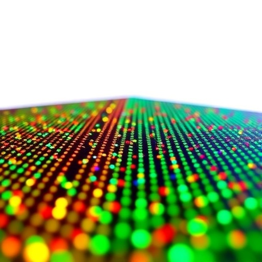
A new advance in quantum-dot (QD) display manufacturing could help push next-generation full-colour electroluminescence (EL) screens toward larger sizes and higher resolution—without relying on toxic cadmium. In a recent study, researchers report a “cracking-assisted transfer printing” (CATP) technology designed to precisely pattern cadmium-free QD light-emitting layers on active-matrix (AM) backplanes.
The core challenge in QD displays is achieving sharp, high-density pixel boundaries while preserving the optical quality of QD films. Traditional patterning approaches often leave residues, damage QDs, or create non-uniform interfaces that reduce photoluminescence quantum yield (PLQY) and can increase leakage currents between pixels. CATP tackles this by using controlled crack formation to enable accurate transfer of QD patterns onto complex substrates.
According to the researchers, CATP provides scalability and geometric versatility, allowing it to print across large areas and onto non-standard backplanes. That includes flexible, stretchable, and even textile-like architectures—categories that are difficult for conventional lithography-based methods. In their demonstrations, the team achieved uniform pixelization on 4-inch substrates, reaching pixel sizes as small as 600 nm.
The method also supports full-colour RGB integration on backplanes with non-planar, uneven surfaces. Importantly, the researchers report minimal cross-contamination between neighbouring RGB pixels, a key requirement for maintaining colour purity and preventing visible artefacts in high-resolution display panels.
A major highlight is a cadmium-free full-colour EL QD display built on an LTPS TFT AM backplane. The prototype delivers 320 × RGB × 360 pixels across a 1.41-inch active area (341 ppi), reaching a colour gamut of 124% for sRGB and 92% for DCI-P3. Beyond rigid devices, the team also fabricated a flexible-format pixelated EL QD display, indicating potential pathways for rollable or wearable visual technologies.
From a performance standpoint, CATP appears to improve electro-optical behaviour and operational lifetime relative to other QD patterning strategies. The authors attribute this to precision “nano-interface” control during transfer, which preserves QD emissive efficiency (enhancing film PLQY) and reduces local current leakage by enabling tighter, more reliable QD packing density.
If validated across longer lifetimes and even larger panel formats, CATP could become a viral-looking enabling technology for high-resolution augmented reality (AR) and virtual reality (VR) displays, where both pixel density and manufacturability are critical bottlenecks. The study suggests that crack-guided transfer could be the missing link between laboratory QD pixel performance and production-ready display architectures.
Cite Scienmag News
Katie Riggs. (July 17, 2026). Cracking-Assisted Transfer Printing Enables High-Resolution Quantum Dot LED Displays. Scienmag. https://scienmag.com/cracking-assisted-transfer-printing-enables-high-resolution-quantum-dot-led-displays/
Katie Riggs. "Cracking-Assisted Transfer Printing Enables High-Resolution Quantum Dot LED Displays." Scienmag, 17 July 2026, https://scienmag.com/cracking-assisted-transfer-printing-enables-high-resolution-quantum-dot-led-displays/. Accessed 3 September 2026.
Katie Riggs. "Cracking-Assisted Transfer Printing Enables High-Resolution Quantum Dot LED Displays." Scienmag. July 17, 2026. https://scienmag.com/cracking-assisted-transfer-printing-enables-high-resolution-quantum-dot-led-displays/


