This study is led by Prof. Xu (State Key Laboratory of Integrated Optoelectronics, College of Electronic Science and Engineering, Jilin University), Prof. Yu (College of Information Science and Electronic Engineering, Zhejiang University), Prof. Han (Precision Instrument and Optoelectronics Engineering, Key Laboratory of Optoelectronic Information Technology, Tianjin University and Guangxi Key Laboratory of Optoelectronic Information Processing, School of Optoelectronic Engineering, Guilin University of Electronic Technology), and Prof. Sun (State Key Laboratory of Integrated Optoelectronics, College of Electronic Science and Engineering, Jilin University and State Key Laboratory of Precision Measurement Technology and Instruments, Department of Precision Instrument, Tsinghua University).

Credit: ©Science China Press
This study is led by Prof. Xu (State Key Laboratory of Integrated Optoelectronics, College of Electronic Science and Engineering, Jilin University), Prof. Yu (College of Information Science and Electronic Engineering, Zhejiang University), Prof. Han (Precision Instrument and Optoelectronics Engineering, Key Laboratory of Optoelectronic Information Technology, Tianjin University and Guangxi Key Laboratory of Optoelectronic Information Processing, School of Optoelectronic Engineering, Guilin University of Electronic Technology), and Prof. Sun (State Key Laboratory of Integrated Optoelectronics, College of Electronic Science and Engineering, Jilin University and State Key Laboratory of Precision Measurement Technology and Instruments, Department of Precision Instrument, Tsinghua University).
The terahertz band is a gap band between microwave and infrared, and has shown great application potential in many cutting-edge information fields such as 6G communications. Terahertz silicon-based photonics has many advantages such as high transmission efficiency and is an effective platform for realizing terahertz devices. However, how to implement devices with richer functions in the terahertz band or expand device control capabilities is still a hot research topic in terahertz integrated photonics.
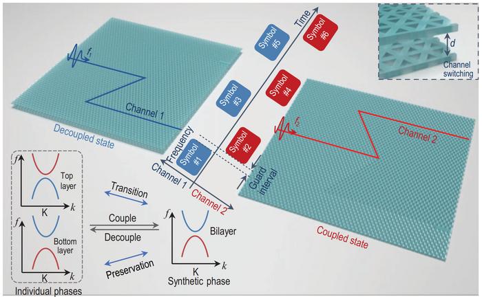
In this study, the author proposed a chip design method based on topological interlayer coupling regulation. This method uses the interlayer coupling strength of the bilayer valley photonic crystal to regulate the Hamiltonian of the bilayer topological photonic system:
H = HT + HB + HTB
Where HT and HB represent the Hamiltonian of the top and bottom photonic lattice respectively, while HTB is used to describe the Hamiltonian generated due to interlayer coupling. By regulating the distance between layers, the system can be effectively controlled to be in a coupled state or a decoupled state, and the interlayer coupling Hamiltonian HTB can be adjusted to control the topological phase transitions of the photonic system. Due to the bulk-edge correspondence, the topological edge states before and after the phase transition can be distributed in different spatial paths. Through modular topological phase design, the author realized the flexible multiplexing chip shown in Figure 1.
In order to verify the potential application value of the technical solution in next-generation communications, the research team conducted relevant tests on the terahertz communication performance of the chip (Figure 2.a). The multiplexing chip achieves 10 Gbps and 12 Gbps 16-QAM signal transmission on two switchable channels of 120 GHz and 130 GHz respectively, with available bandwidths of 2.5 GHz and 3 GHz respectively (Figure 2.b).
This work enriches the methods of terahertz on-chip channel manipulation, further promotes the application of topological photonics in advanced communication systems and devices, and may inspire more novel physical mechanisms and phenomena in bilayer and multi-layer topological systems.
See the article:
Design of the topological photonic lattices, Simulation results, and measured S-parameters.
Journal
National Science Review


