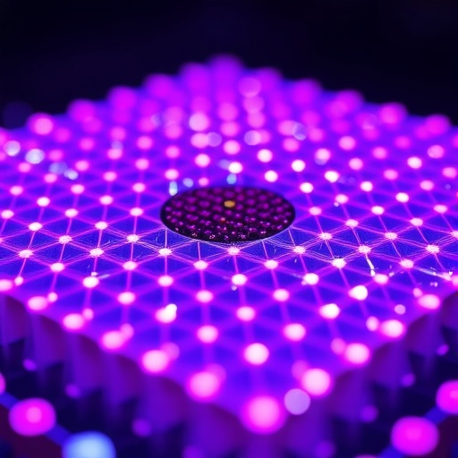
Recent advancements in the field of photonic integration are revolutionizing how we manage and manipulate light on small scales. As the demand for high-speed, dynamic light control increases, scientists are turning to innovative solutions to push the boundaries of what’s possible with existing technologies. One particularly exciting development comes from research into metasurfaces, which are engineered materials that can manipulate light in ways that were, until recently, thought to be impossible. These structures are paving the way for the next generation of integrated photonic devices, promising unprecedented levels of information processing capability and operational flexibility.
Metasurfaces operate at the subwavelength scale, meaning they can manipulate light with a precision that surpasses traditional optical components. This dynamic capability allows the integration of metasurfaces with optical waveguides, facilitating the coupling of on-chip signals into free space with multi-dimensional control. The potential applications of these technologies are vast, ranging from simple optical components to highly complex multifunctional devices capable of dynamic holographic displays. However, two significant challenges have marred the effectiveness of current on-chip metasurfaces: the need for dynamic tunability and the limitations on information capacity.
The optical properties of most existing metasurfaces are typically fixed post-fabrication, meaning that adjustments to their performance are challenging to accomplish in real-time. While various modulation methods have been explored, such as those using liquid crystals, these techniques tend to exhibit slow response rates and limited control over individual pixels. Consequently, the movement towards real-time, dynamic control of light fields has been stymied by these technological limitations. Moreover, current multiplexing techniques struggle to meet the demands of high-throughput optical information processing, highlighting the urgent need for innovative approaches to enhance the functionality and capacity of optical devices.
In a notable study published in Light: Science & Applications, researchers led by Professor Tao Li from Nanjing University have made significant strides toward overcoming these challenges. Their work presents a unique modulation strategy utilizing a lithium niobate on insulator (LNOI) platform, which houses an advanced on-chip metasurface designed for both fast response times and improved multiplexing capabilities. By employing a diatomic on-chip integrated metasurface as an addressing unit, the team ingeniously combined geometric and detour phase mechanisms to enhance performance dramatically.
Their innovative design enables the contrivance of a four-channel multiplexing system, effectively allowing independent control over illumination direction and polarization states. Such advancements present clear benefits for information capacity, empowering the integration of multiple data streams simultaneously. An important aspect to consider is that these on-chip metasurfaces harness the capabilities of waveguides via a network architecture, providing a scalable and adaptable framework ideal for multi-channel multiplexing applications. By leveraging waveguide crossing arrays, researchers are not only enhancing performance but opening new avenues for localized and addressable manipulation of light fields.
Dynamic tunability is achieved by utilizing the rapid advancements in lithium niobate technology, a material known for its excellent electro-optical properties. Thin-film lithium niobate has emerged as a significant platform for the construction of next-generation photonic integrated chips. The effective use of lithium niobate electro-optical modulators enriches the on-chip metasurface network by introducing rapid response capabilities, enabling nanosecond-level light field modulation. This process allows for exceptionally high-speed optical routing, effectively directing signals to selected input ports based on applied voltages.
In the study’s experimental setup, an electro-optical switch composed of three lithium niobate modulators stands at the core of their innovation. This switch functions as a high-speed optical router, facilitating precise control over the activation of various units within the metasurface network. This novel capacity ensures that users can swiftly and dynamically call up desirable holographic images, improving the user experience in applications such as optical communication and display technologies. The practical implications of such rapid switching capabilities were showcased through the theoretical demonstration of dynamic holographic letters, effectively illustrating the interface between light manipulation and data representation.
The work of Professor Li’s team extended the functionality of single metasurfaces by expanding into a 2×2 network structure on a waveguide crossing array. This advancement introduces flexibility in designing optical systems, where specific unit activations can lead to diverse holographic displays based on adjusted incident ports. The inherent scalability of this architecture positions it as a promising solution for high-density, large-capacity optical information storage and processing, essential for the demands of modern technology.
As researchers continue to explore the possibilities inherent in metasurface technology, the findings from this study underscore a crucial evolution in the realm of optical manipulation. The integration of these devices within photonic systems opens multiple pathways for future research and application, especially as the demand for efficient and rapid information processing escalates. The convergence of dynamic, programmable metasurfaces with advanced materials like lithium niobate suggests a fruitful direction for ongoing investigations, heralding a new era of photonic capabilities that will likely underpin the next generation of optical devices.
In summary, the transformative research conducted by Professor Tao Li and his collaborators highlights a significant step toward mitigating the limitations that have historically hampered on-chip metasurfaces. The efforts illustrated in their study not only broaden our understanding of light manipulation techniques but also set the stage for innovative applications that could have far-reaching consequences across a range of domains, from telecommunications to advanced holographic display systems. Through a combination of ingenuity and state-of-the-art materials science, their work lays down foundational knowledge that future researchers can build upon as the field of integrated photonics continues to evolve.
As we peer into the future of photonics, it’s clear that the groundbreaking advances achieved by these scientists will likely play a pivotal role in shaping the technologies that drive our increasingly interconnected and data-driven society. The intersection of materials science, optics, and engineering that defines this research represents a critical juncture, where the potential for discovery is limited only by our imagination and commitment to exploring the multifaceted nature of light.
Subject of Research: Dynamic holographic display with addressable on-chip metasurface network
Article Title: Dynamic holographic display with addressable on-chip metasurface network based on lithium niobate photonics
News Publication Date: [Publication Date Not Provided]
Web References: [Reference Not Provided]
References: [Reference Not Provided]
Image Credits: Zhizhang Wang et al.
Keywords
Metasurfaces, photonic integration, lithium niobate, dynamic light manipulation, holographic displays, electro-optical modulation, information processing.
