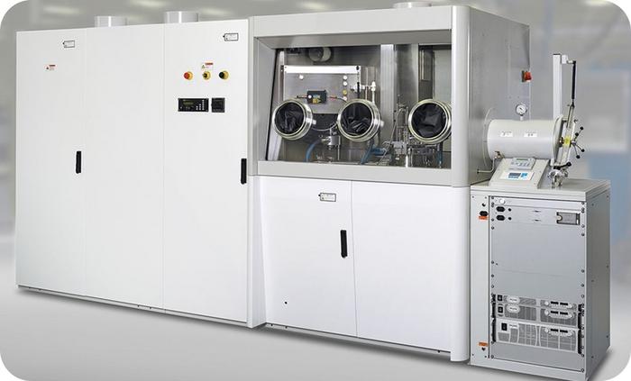
South Korean researchers have successfully developed technology to mass-produce quantum dot lasers, widely used in data centers and quantum communications. This breakthrough paves the way for reducing the production cost of semiconductor lasers to one-sixth of the current cost.

Credit: Electronics and Telecommunications Research Institute(ETRI)
South Korean researchers have successfully developed technology to mass-produce quantum dot lasers, widely used in data centers and quantum communications. This breakthrough paves the way for reducing the production cost of semiconductor lasers to one-sixth of the current cost.
Electronics and Telecommunications Research Institute (ETRI) announced that they have developed, for the first time in Korea, technology to mass-produce quantum dot lasers, previously only used for research, using Metal-Organic Chemical Vapor Deposition (MOCVD) systems.
The ETRI Optical Communication Components Research Section has successfully developed indium arsenide/gallium arsenide (InAs/GaAs) quantum dot laser diodes on gallium-arsenic (GaAs) substrates, which are suitable for the 1.3 µm wavelength band1) used in optical communications.
1) Optical Communication Wavelength Band (1260~1360nm)
Traditionally, quantum dot laser diodes were produced using Molecular Beam Epitaxy (MBE), but this method was inefficient due to its slow growth speed, making mass production challenging. By utilizing MOCVD, which has higher production efficiency, the research team has significantly enhanced the productivity of quantum dot laser manufacturing. Quantum dot lasers are known for their excellent temperature characteristics and strong tolerance to substrate defects, allowing for larger substrate areas and consequently lower power consumption and production costs.
The newly developed quantum dot manufacturing technology boasts high density and good uniformity. The produced quantum dot semiconductor lasers demonstrated continuous operation at temperatures up to 75 degrees Celsius, showing a world-leading achievement in the results obtained via MOCVD.
Previously, optical telecommunication devices used expensive 2-inch indium phosphide (InP) substrates, resulting in high manufacturing costs. The new technology, using GaAs substrates, which are less than one-third the cost of InP substrates, is projected to reduce the manufacturing cost of communication semiconductor lasers to less than one-sixth.
This technology’s ability to use large-area substrates enables significant reductions in process time and material costs.
The research team plans to further optimize and verify this technology to enhance its reliability and transfer it to domestic optical communication companies. These companies will receive key technology and infrastructure support through ETRI’s semiconductor foundry, accelerating the commercialization timeline.
The anticipated reduction in development time and production costs will enhance product price competitiveness, potentially increasing market share internationally. This advancement is expected to boost the domestic optical communication component industry.
In modern society, optical communication serves as the backbone of our industry. The research team’s achievement is set to revolutionize the development of optical sources, connecting apartment complexes to large cities and undersea optical cables.
Professor Dae Myung Geum from Chungbuk National University, a participant in this research, remarked, “The mass production technology for quantum dots can significantly lower the production costs of high-priced optical communication devices, enhancing the competitiveness of the national optical communication component industry and contributing substantially to basic science research.”
Dr. Ho Sung Kim from ETRI’s Optical Communication Components Research Section stated, “This research outcome is a prime example of securing both commercial viability and fundamental innovation, potentially changing the paradigm of the semiconductor laser industry for optical communications.”
###
This achievement was made possible through ETRI’s basic project, “ICT Creative Technology Development,” and has been published in a recent international SCI journal2).
2) SCI Journal Article Title: “High-temperature continuous wave-operation of all MOCVD grown InAs/GaAs quantum dot laser diodes with highly strained InGaAs layer and low temperature p-AlGaAs cladding layer” – Top 10%, “Journal of Alloys and Compounds”, 983(2024) 173823 (JCR IF 6.2)
About Electronics and Telecommunications Research Institute (ETRI)
ETRI is a non-profit government-funded research institute. Since its foundation in 1976, ETRI, a global ICT research institute, has been making its immense effort to provide Korea a remarkable growth in the field of ICT industry. ETRI delivers Korea as one of the top ICT nations in the World, by unceasingly developing world’s first and best technologies.
Journal
Journal of Alloys and Compounds
Article Title
High-temperature continuous wave-operation of all MOCVD grown InAs/GaAs quantum dot laser diodes with highly strained InGaAs layer and low temperature p-AlGaAs cladding layer
Article Publication Date
1-May-2024


