Researchers at Columbia Engineering have embarked on a revolutionary undertaking that sees DNA being utilized to create three-dimensional electronic devices characterized by nanometer-scale features. This groundbreaking method stands to transform the field of electronics, particularly through enhancing the power and density of microchip assemblies. By harnessing the unique self-assembling properties of DNA, the team has developed an innovative manufacturing technique that could pave the way for high-performance computing and advanced artificial intelligence systems that better mimic the structural intricacies of the human brain.
This shift from traditional two-dimensional circuit design to a three-dimensional architecture is not merely an aesthetic upgrade; it signifies a substantive leap in the potential capacity for data processing and storage. Oleg Gang, the leading researcher and Professor of Chemical Engineering and Applied Physics at Columbia, emphasizes the importance of this advancement. As he articulates, 3D electronic structures have the potential to outperform their 2D counterparts significantly. Gang’s insights, rooted in his position at the Center for Functional Nanomaterials at Brookhaven National Laboratory, illuminate the possible implications of this evolution within the realm of technology.
The current landscape of electronics is dominated by flat circuitry, a methodology that imposes constraints on the efficacy and potential of electronic devices. Traditional manufacturing processes are typically carried out in a top-down approach, where complex structures are carved from blocks of material through methods akin to sculpting. Although these techniques have been the mainstay in electronics manufacturing, they encounter severe limitations. The challenges of developing advanced 3D structures economically and efficiently, while managing the accumulation of errors through numerous steps, render these traditional methods inadequate for the demands of modern technology.
In contrast to the top-down approach, the innovative techniques developed by Columbia Engineering aim to construct electronic frameworks from the bottom up. This biologically inspired methodology utilizes self-assembling principles that allow for the creation of intricate 3D designs using DNA. The researchers’ pioneering work leverages the unique folding capabilities of DNA strands that can naturally arrange themselves into specific shapes, resembling biological origami. By doing this, they have successfully demonstrated that complex 3D frameworks can be assembled with incredible precision at the nanoscale.
The DNA strands are constructed from four basic nucleotide building blocks—adenine (A), thymine (T), cytosine (C), and guanine (G)—which exhibit strong, defined pairing properties. The intricacies of this molecular interaction enable many engineered DNA strands to fold into desired shapes after being programmed with specific sequences. Such adaptability allows researchers to create customized structures that act as wire-like scaffolds for electronic components, culminating in devices capable of integrating diverse functionalities.
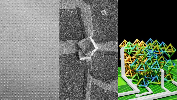
In this innovative study, the accomplished first author, Aaron Michelson, alongside his colleagues, set out to explore the feasibility of anchoring small pieces of DNA onto a gold-coated substrate. This foundational step was critical, as the attached DNA sequences served as anchors for octahedral DNA frames, which could spontaneously assemble into larger 3D frameworks at predetermined locations. This ingenious strategy not only ensured the creation of complex structures but also allowed for better spatial organization—a significant aspecto when considering scalability in electronic manufacturing.
The experiments progressed as the team scaled up their designs, collaborating with experts from the University of Minnesota to enhance their 3D scaffolds’ practicality. Once the DNA frameworks were in place, the researchers coated them with silicon oxide and infused the structures with tin oxide, a semiconductor. Electrodes were then strategically connected to each 3D device, forming light sensors that exhibited electrical responses upon exposure to illumination. This remarkable outcome demonstrated that integrating biological self-assembly processes with conventional microchip technology can result in the production of operational devices.
The implications of this research extend beyond simply creating functional electronic devices. As Gang notes, there lies a vision of advancing artificial intelligence architectures that are inspired by the complex neuronal networks found within the human brain. By mimicking the brain’s natural 3D structure, these novel electronic architectures can potentially offer more effective computational capabilities than existing 2D systems. Thus, the proposed methodology holds promise not only for advancing microelectronics but also for influencing broader domains, including the future of artificial intelligence.
As the Columbia researchers reflect on their achievements, they recognize that the journey is far from over. The immediate focus is on leveraging this self-assembling technique to fabricate increasingly sophisticated electronic devices that capitalize upon the ability to combine multiple materials. This ambition speaks to the limitless possibilities lying ahead as researchers like Gang and his team push forward into uncharted territory, laying the groundwork for next-generation circuitry.
In summary, the work being done at Columbia Engineering signifies a paradigm shift in electronic device fabrication, where the implementation of bottom-up assembly techniques through DNA programmability offers a promising avenue towards developing advanced functional devices. The capacity to integrate such designs into microchips combines the precision of biotechnology with the demands of modern electronics, setting the stage for possible breakthroughs that could reshape the industry for years to come.
As the world looks ahead into the horizon of technology, the implications of this research resonate deeply within the scientific community, fueling discussions and igniting enthusiasm about the potential applications that may emerge from this innovative approach. At this intersection of biology and engineering, the possibility of expanding into realms previously considered mere science fiction now feels increasingly tangible, as the foundations for the circuits of the future are being established today.
Ultimately, the work at Columbia Engineering serves as a poignant reminder of the profound interconnectivity of disciplines, urging a collective response not only from scientists and engineers but also from those in philosophical arenas who contemplate the implications of such advancements for society at large. As we journey through this new epoch of technology, the marriage of biology and systems engineering heralds a future imbued with potential—one where the extraordinary is increasingly achievable through the application of creativity, knowledge, and innovation.
Subject of Research: 3D Electronic Devices via DNA Self-Assembly
Article Title: Scalable Fabrication of Chip-Integrated 3D Nanostructured Electronic Devices via DNA-Programmable Assembly
News Publication Date: 28-Mar-2025
Web References: Columbia Engineering
References: Science Advances
Image Credits: Credit: Center for Functional Nanomaterials
Keywords
Applied Sciences, Engineering, Electrical Engineering, Electronics
