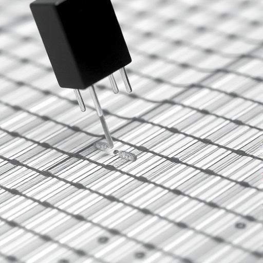
In a groundbreaking advancement within the field of printed electronics, researchers have successfully implemented a novel capillary flow printing technique that enables the fabrication of submicrometre carbon nanotube thin-film transistors. This innovation comes at a crucial time as the demand for miniaturized electronic components continues to surge across various industries, from flexible electronics to IoT devices. The method significantly transcends the limitations of existing printing techniques that rely on resolutions of 10–30 µm, a range that has often hindered the scalability and utility of printed transistors in real-world applications.
Historically, achieving printed transistors with submicrometre channel lengths necessitated complex chemical processes or extensive post-processing, which inherently restricted their applicability in practical settings. This new methodology, however, appears to sidestep such convolutions, allowing for direct fabrication without the need for chemical alterations or physical interventions after printing. This not only streamlines the production process but also opens up possibilities for using the technology in diverse applications, thereby enhancing its overall versatility.
Capillary flow printing operates by exploiting the natural tendency of liquids to move through narrow spaces. In this innovative approach, researchers have successfully utilized this property to print various conducting, semiconducting, and insulating inks onto a plethora of substrate materials including silicon, Kapton, and paper. The research team demonstrated that the technology is not merely limited to a single type of substrate but can adapt to various surfaces, expanding the range of potential applications significantly.
When examining the performance of the fabricated carbon nanotube thin-film transistors, the results were nothing short of impressive. The devices exhibited on-currents of 1.12 mA mm−1 when operating through a back-gated configuration on a Si/SiO2 substrate. Furthermore, when the transistors were side-gated using an ion gel on Kapton, the on-current registered at a respectable 490 µA mm−1. Such results indicate that the electrical performance of these printed transistors is quite competitive, potentially rivaling traditionally manufactured counterparts.
Moreover, a key feature of this research is the assessment of mechanical resilience. The transistors printed on Kapton substrates displayed exceptional properties in terms of mechanical bending and sweep rate resilience. This characteristic is particularly vital, as flexible electronics are increasingly becoming integral components in personal electronics and wearable technologies. The ability to maintain performance integrity under physical stress is a crucial metric for evaluating the feasibility of these printed devices in real-world applications.
The capillary flow printing approach not only makes the printed devices functionally innovative but also positions itself as a sustainable solution within the context of manufacturing. Traditional methods of fabricating transistors are often resource-intensive, requiring significant energy, materials, and time. By contrast, capillary flow printing offers a more efficient route to producing high-quality transistors, which could lead to reduced waste and a lower carbon footprint in the long run.
Furthermore, the implications of this breakthrough extend beyond individual devices and could reshape entire electronic systems. As the ability to create highly functional, submicrometre transistors that are both flexible and robust becomes more accessible, industries involved in electronics manufacturing may find themselves at a pivotal junction where cost-effective, scalable solutions become standard practice.
Analyzing the broader impact, one cannot overlook how this technology could facilitate the development of next-generation electronics. As high-performance printed transistors become a reality, we might witness a significant leap in the capabilities of flexible and portable electronic devices. This is particularly promising for applications in areas such as health monitoring, where lightweight and flexible electronics can enhance patient comfort and device functionality.
In addition to health technology, this innovation has potential implications in sectors like automotive and consumer electronics. Imagine the prospects of flexible displays that could bend and adapt to various forms without compromising their functionalities, or intelligent wearable devices embedded with these high-performance transistors, continuously monitoring and responding to user needs. The versatile applications of capillary flow printed transistors could redefine product design and consumer experiences in multiple domains.
While the research undoubtedly demonstrates exciting possibilities, the team acknowledges the continuous challenges that must be addressed for widespread adoption. Scaling the technology for mass production while maintaining the same high-performance standards will be a critical next step. Collaborative efforts between academia and industry may accelerate this process, ultimately leading to commercialization opportunities that capitalize on this innovative printing technique.
Looking ahead, it will be essential to explore further advancements in ink formulations, substrate compatibility, and printing techniques to expand the range of materials and applications. With continued research and development, we may witness an evolution within the realm of printed electronics that aligns with future demands and technological aspirations.
As the world increasingly gravitates towards miniaturization and portability in electronics, capillary flow printing emerges as a vital player. This new technique not only breaks the barriers imposed by conventional printing technologies but also paves the way for an exciting future where printed electronics can seamlessly blend into our daily lives. The forthcoming years will undoubtedly unveil more such innovations, with the potential to revolutionize how we interact with technology and redefine what is possible in the fascinating field of electronics.
In conclusion, the study conducted by Smith et al. elucidates a pivotal moment in the domain of printed electronics. The successful demonstration of capillary flow printing for fabricating submicrometre carbon nanotube transistors signals a substantial leap forward. As this promising technology continues to evolve, the obstacles of traditional manufacturing processes may soon become relics of the past, providing exciting new avenues for research, development, and ultimately, commercialization in the dynamic landscape of electronics.
Subject of Research: Capillary flow printing of submicrometre carbon nanotube thin-film transistors.
Article Title: Capillary flow printing of submicrometre carbon nanotube transistors.
Article References:
Smith, B.N., Albarghouthi, F.M., Doherty, J.L. et al. Capillary flow printing of submicrometre carbon nanotube transistors.
Nat Electron (2025). https://doi.org/10.1038/s41928-025-01470-7
Image Credits: AI Generated
DOI:
Keywords: carbon nanotubes, thin-film transistors, capillary flow printing, flexible electronics, submicrometre fabrication, printed electronics, sustainable manufacturing, high-performance devices, innovative technology, electronic systems.


