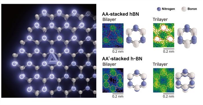
Researchers from the Pohang University of Science and Technology (POSTECH) in South Korea, alongside their collaborators at the University of Montpellier in France, have made a groundbreaking advancement in the synthesis of hexagonal boron nitride (hBN). This innovative research, detailed in the prestigious journal Nature Materials, unveils the successful creation of wafer-scale hBN exhibiting an AA-stacking configuration. This crystal structure is significant because it was previously deemed unattainable in laboratory conditions, where stacking arrangements critically influence the material’s electronic properties.
The synthesis process utilized in this research involved cutting-edge metal-organic chemical vapor deposition (MOCVD) techniques on a gallium nitride (GaN) substrate, which is known for its abrupt crystalline structure and compatibility with two-dimensional materials. The research team employed a meticulous method where they arranged the layers of hBN in an AA configuration, where identical atoms line up directly as opposed to the more unstable AA’ configuration where boron and nitrogen atoms alternate. This spatial arrangement is crucial for enhancing the material’s insulating properties, which are essential in a range of future electronic applications.
As the researchers conducted their experiments, they discovered that step-edges on the vicinal GaN substrates served as pivotal nucleation sites. These step-edges played a fundamental role in guiding the growth of hBN layers, effectively promoting their unidirectional alignment while reducing any rotational disorder. This remarkable step-edge guided growth mechanism enabled the team to produce high-quality AA-stacked hBN films that maintained an exceptional level of structural uniformity and crystallinity. Such characteristics are vital for the successful integration of hBN into next-generation electronic and photonic devices.
Another significant aspect of this research is the influence of charge incorporation as a result of carbon doping during the MOCVD process. The addition of carbon atoms into the hBN lattice effectively altered the interactions between layers, creating excess charge carriers that mitigated the strong interlayer electrostatic repulsion that typically destabilizes the AA stacking configuration. Hence, this innovative approach does not only demonstrate a new stacking technique but also introduces a previously unconsidered mechanism for tuning the properties and stacking order of van der Waals materials efficiently.
The theoretical assumptions governing the stacking configurations of van der Waals materials have been substantially challenged by this study. For years, scientists have operated under the belief that stacking arrangements in materials like hBN are predominantly controlled by thermodynamic preferences. However, Professors Jong Kyu Kim and Si-Young Choi from POSTECH, along with Guillaume Cassabois from the University of Montpellier, assert that the characteristics of the substrate and the inclusion of charge carriers are equally influential. Such revelations expand the horizons for customizing the architectures of two-dimensional materials, allowing for the engineering of materials with distinct and targeted electronic and optical properties.
Subsequent optical characterization of the synthesized AA-stacked hBN films revealed heightened second-harmonic generation (SHG), which serves as a hallmark for identifying non-centrosymmetric crystal structures. The implications of this feature are wide-ranging, pointing towards its applications in nonlinear optics, which has been an area of intense research interest due to the unique properties offered by such materials. Moreover, the material exhibited sharp band-edge emissions in the deep-ultraviolet (DUV) region, indicating its applicability in developing high-efficiency optoelectronic devices.
The implications of achieving wafer-scale control over the stacking order of hBN are substantial for the future of scalable, high-performance electronic and photonic systems. Seokho Moon, a postdoctoral researcher in Professor Kim’s lab and the lead author of the study, emphasized the importance of their findings by noting that the ability to precisely engineer stacking configurations is a significant step forward. This ability not only enhances the understanding of two-dimensional materials but also opens new pathways for research into their implementation in functional devices.
Furthermore, the funding backing this pioneering research demonstrates a commitment to advancing material science technologies. The research was supported by several programs including the Global Ph.D. Fellowship Program and the Basic Science Research Capacity Enhancement Program by the Ministry of Education, as well as other initiatives from the Ministry of Science and ICT, and Samsung Electronics. This collaborative effort showcases the importance of cross-institutional and governmental support in leading to discoveries that redefine the boundaries of materials engineering.
The synthesis of wafer-scale AA-stacked hBN presents a significant breakthrough in the field of materials science, particularly in the engineering of van der Waals materials. Understanding the mechanisms behind stacking configurations and how they can be manipulated opens a new frontier for research and application in various sectors, including quantum computing, advanced electronic devices, and photonic technologies. This work illustrates how the integration of fundamental science with innovative engineering techniques can create transformative effects in the world of nanomaterials, potentially leading to improvements in the performance and capability of future technologies.
In summary, the successful synthesis of wafer-scale AA-stacked hBN represents not just a scientific accomplishment but a pivotal moment in the exploration of new materials with tailored functionalities. The insights gained from this research contribute significantly to our understanding of two-dimensional materials, promising to spur advances across industries reliant on both electronic and optical applications in their future developments.
Subject of Research: Synthesis of wafer-scale hexagonal boron nitride with AA-stacking configuration
Article Title: Wafer-scale AA-stacked hexagonal boron nitride grown on a GaN substrate
News Publication Date: 19-Mar-2025
Web References: http://dx.doi.org/10.1038/s41563-025-02173-2
References: Nature Materials
Image Credits: Credit: POSTECH
Keywords: hexagonal boron nitride, AA-stacking configuration, metal-organic chemical vapor deposition, van der Waals materials, optoelectronics, quantum photonics, nanoscale materials, electronic devices, crystal structure, photonic systems, non-centrosymmetric crystal structures, deep ultra-violet region.


