In the ever-evolving landscape of semiconductor technology, the race toward smaller, faster, and more efficient transistors continues unabated. At the forefront of this pursuit are gate-all-around metal-oxide-semiconductor field-effect transistors (GAA MOSFETs), which represent a cutting-edge architecture promising enhanced electrostatic control and superior channel modulation. While these nanoscale devices hold immense potential for future integrated circuits, simulating their behavior accurately and efficiently remains a formidable challenge due to their complex three-dimensional geometries and the intricate physics governing carrier transport. A new study conducted by Lee, Kim, Jung, and colleagues introduces a groundbreaking methodology that combines quasi-one-dimensional (quasi-1D) modeling with region-wise structural analysis, heralding a significant leap forward in technology computer-aided design (TCAD) simulations.
Traditional TCAD simulation approaches often rely on solving full three-dimensional partial differential equations to model semiconductor devices, a process that is both computationally intensive and time-consuming. This complexity sharply escalates when dealing with GAA MOSFETs because their architecture involves multiple vertically stacked nanowires or nanosheets wrapped by a gate, resulting in nontrivial electrostatics and charge distribution profiles. Lee and team’s innovative quasi-1D modeling approach cleverly sidesteps the computational bottleneck by reducing the dimensionality of the problem without compromising the accuracy of key physical parameters.
The crux of their approach lies in deconstructing the transistor structure into multiple regions, each exhibiting distinct physical behaviors, and applying tailored models to these discrete sections. By employing region-wise analysis, the model captures the local variations in electrostatics, charge density, and potential distribution by solving coupled quasi-1D equations along relevant device axes. This method enables the simulation framework to achieve rapid convergence and significantly lower computational loads, while still yielding high-fidelity results that align closely with full-scale three-dimensional simulations and experimental measurements.
One of the pivotal advancements of this framework is its nuanced treatment of the gate-all-around geometry, which is notoriously difficult to model due to the surround gate encasing the channel from all sides. By partitioning the device cross-section and applying geometry-specific boundary conditions and material parameters, the researchers meticulously capture the multi-dimensional effects in an effectively reduced-dimensional simulation environment. This approach preserves the essential electrostatic coupling and quantum confinement effects that dominate transistor operation at such nanoscale regimes.
Moreover, the proposed methodology streamlines the inclusion of key physical phenomena such as carrier transport within the inversion layer, short channel effects, and series resistance contributions without resorting to overly complex or non-physical approximations. Such fidelity ensures that predictive power is maintained, which is crucial for device engineers who depend on accurate simulations for design optimization and process development in advanced semiconductor manufacturing.
The implications of this research extend beyond mere computational efficiency. By enabling rapid and reliable simulations of GAA MOSFETs, the quasi-1D region-wise modeling technique accelerates the iterative design cycle, allowing researchers and engineers to explore broader design spaces with greater confidence and without prohibitive computational expense. This capability is invaluable as the semiconductor industry strives to push device geometries to their physical and practical limits, especially in the context of scaling and energy-efficient architectures.
In practical terms, the study demonstrates how the proposed framework adeptly handles the parameter sweeps commonly required in device design, such as varying gate lengths, oxide thicknesses, doping profiles, and channel materials. The reduction in simulation time opens the door to high-throughput virtual prototyping, thereby slashing the development timelines associated with next-generation transistor technologies.
The collaborative nature of this cross-disciplinary work deserves recognition, as it brings together deep expertise in semiconductor physics, numerical methods, and computational science. This synergy has yielded a tool that not only pushes the envelope in device modeling but also holds promise for adaptability to other nanoscale device architectures, potentially including finFETs, nanowire sensors, and emerging quantum devices.
Critically, the research stresses validation through benchmarking against both experimental data and full 3D TCAD simulations, establishing confidence in the approach and its predictions. Such rigorous evaluation underscores the maturity of the quasi-1D modeling technique and its readiness for integration into mainstream device design workflows.
Looking toward the future, this research could catalyze further innovations in TCAD methodologies. The principles underlying the region-wise quasi-1D approach might be extended to handle even more complex material heterostructures, multigate arrangements, or 2D semiconductor layers, which are rapidly gaining traction in the semiconductor research community.
The adoption of this simulation paradigm could also dovetail with machine learning strategies, where rapid simulation outputs feed into training data for surrogate models or optimization algorithms, ultimately fostering even more powerful and agile design platforms.
Furthermore, as GAA MOSFETs inch closer to mass production and commercialization, tools like the one presented by Lee and colleagues will become indispensable for reliably predicting device behaviors under various operating conditions and process variations, thus ensuring robust yield and performance in industrial settings.
In sum, the integration of quasi-1D modeling with region-wise structural analysis represents a vital breakthrough in semiconductor device simulation. It exemplifies how innovative modeling strategies can overcome longstanding challenges imposed by device miniaturization and architectural complexities, underpinning the continued evolution of advanced transistor technologies that power the digital world.
The significance of this development resonates across academia and industry alike, promising a new era of rapid, accurate, and scalable TCAD simulation capabilities. As the semiconductor roadmap advances, methodologies such as these will be critical enablers, ensuring that design innovation keeps pace with physical and economic constraints.
This pioneering work by Lee, Kim, Jung, and their team is poised to become a cornerstone in the modeling toolbox for GAA MOSFETs and potentially beyond, illustrating the profound impact that intelligent dimensionality reduction and region-specific analysis can have on solving complex engineering problems.
Their full study, published in Communications Engineering, offers detailed insights into the mathematical formulations, computational validations, and practical applications of this method, setting a benchmark for future research in the domain.
By addressing fundamental computational barriers without sacrificing physical accuracy, this study charts a compelling path to accelerating the next-generation semiconductor device design and underscores the vital role of inventive modeling in technological progress.
Subject of Research:
Gate-All-Around (GAA) MOSFET simulation methodologies.
Article Title:
Combining quasi-one-dimensional modeling with region-wise structure analysis for rapid technology computer-aided design simulations of gate-all-around MOSFETs.
Article References:
Lee, KW., Kim, I.K., Jung, SW. et al. Combining quasi-one-dimensional modeling with region-wise structure analysis for rapid technology computer-aided design simulations of gate-all-around MOSFETs. Commun Eng 4, 165 (2025). https://doi.org/10.1038/s44172-025-00509-z
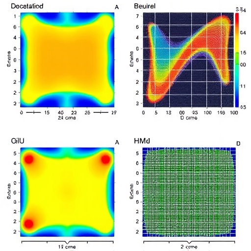
Image Credits: AI Generated
