


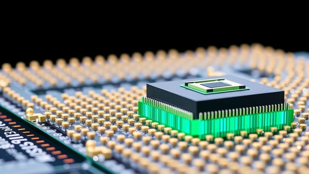
For decades, the semiconductor industry has relied on a simple recipe: shrink transistors, pack them more densely onto flat silicon wafers, and let the resulting density gains drive progress in computing. That recipe is now running into fundamental physical and economic walls. A team of researchers at Purdue University reports a major step toward a different path forward, demonstrating the monolithic three-dimensional integration of atomic-layer-deposited indium oxide semiconductor devices across full 200-millimeter silicon wafers. The work, published in Nature Nanotechnology, shows that more than 100,000 functioning transistors can be stacked vertically in multiple tiers directly on top of one another, using processes compatible with the back-end-of-line steps of a standard complementary metal–oxide–semiconductor foundry flow.
Monolithic 3D integration differs from the chip-stacking approaches used in today’s advanced packaging. Instead of fabricating separate dies and bonding them together with relatively coarse interconnects, monolithic 3D integration builds successive device layers sequentially on the same wafer. Each new tier of transistors is grown and patterned directly on top of the interconnect stack of the tier below. This allows extremely dense vertical connections between logic and memory, dramatically shortening the distances data must travel and opening the door to computing architectures in which memory and processing are woven together in three dimensions. The obstacle has always been thermal budget: conventional silicon processing requires temperatures that would destroy the metal interconnects and devices already in place beneath a new layer, so any channel material added on top must be deposited and processed at low temperatures.
The Purdue team, led by Peide D. Ye of the Elmore Family School of Electrical and Computer Engineering, turned to indium oxide deposited by atomic layer deposition, a technique in which the semiconductor film grows one atomic layer at a time through self-limiting surface reactions. Atomic layer deposition offers exceptional thickness control and superb conformality across large substrates, and the resulting amorphous indium oxide films can be processed at temperatures well within the tolerance of back-end-of-line metallization. Because the films are amorphous rather than crystalline, they sidestep the grain-boundary and lattice-matching problems that plague many alternative low-temperature channel materials, including two-dimensional semiconductors that have attracted enormous attention for the same application.
The demonstration is remarkable for its breadth of device functionality. On the 200-millimeter wafers, the researchers fabricated three tiers of devices spanning ferroelectric field-effect transistors for non-volatile memory, as well as enhancement-mode and depletion-mode field-effect transistors for logic. Ferroelectric transistors hold their stored state without power, enhancement-mode devices switch off cleanly at zero gate voltage, and depletion-mode devices conduct by default, so together they form a complete transistor toolkit suitable for real circuit design. The electrical statistics across the wafers are equally notable. Threshold voltage standard deviations as low as 0.04 volts were achieved, a level of uniformity that rivals commercial silicon devices and indicates that the low-temperature process is genuinely manufacturable rather than a laboratory curiosity. Average electron mobilities reached up to 91.6 square centimeters per volt-second, high enough to support fast switching and strong drive currents in dense vertical layouts.
Uniformity at wafer scale is arguably the central achievement here. Research groups have previously shown promising oxide semiconductor transistors on small chip-scale samples, but moving to a 200-millimeter platform subjects every device to the same statistical scrutiny that foundry engineers apply to silicon. The team systematically characterized how processing variations, including annealing temperatures and capping steps, affected each device family. They found that a surface-capping layer followed by a 300-degree-Celsius anneal substantially improved bias stability, suppressing the threshold voltage drift that can undermine reliability during sustained operation. Statistical distributions of subthreshold swing, threshold voltage, and memory window remained tight across hundreds of measured devices per condition, with sample sizes running into the hundreds for each device type tested.
Thermal robustness was verified layer by layer. Because each tier of devices must survive the processing of the tiers fabricated above it, the researchers subjected finished transistors to the full thermal sequence and re-measured them. Mobility, threshold voltage, and subthreshold characteristics were preserved with negligible shift after the complete stack processing, confirming that indium oxide can endure the cumulative thermal exposure of a multi-tier build. The team also engineered the channel thickness to select device behavior: thinner films of about 1.5 nanometers yielded enhancement-mode operation, while thicker films near 3.0 nanometers produced depletion-mode devices, giving circuit designers the complementary options they need for power-efficient logic within the same material system.
With three functional tiers established, the researchers went beyond device statistics and demonstrated fully functional cross-tier circuits, in which signals travel vertically through inter-tier vias connecting transistors on different layers. This vertical wiring capability is what transforms stacked transistors from a density trick into a genuine architectural opportunity. Logic and memory separated by microns of horizontal wiring in a conventional planar chip can instead sit directly atop one another, connected by short vertical links. The team used a custom process design kit built around compact models of their indium oxide transistors, including a standard cell library of eleven logic gates verified through D flip-flop simulations, to bridge the gap between measured device behavior and large-scale circuit design.
The system-level payoff was quantified in the design of a four-tier 3D computing-in-memory accelerator targeting large-language-model workloads. Computing-in-memory architectures perform matrix operations directly inside memory arrays, sidestepping the energy cost of shuttling data between separate memory and processor units, a bottleneck that dominates the power budget of modern artificial intelligence systems. By vertically interleaving logic and memory tiers made from the same low-temperature oxide platform, the proposed accelerator exploits the short inter-tier connections that monolithic integration uniquely enables. Benchmark simulations showed speed-ups of 1.4 times to 2.9 times over comparable two-dimensional baselines, together with comparable improvements in energy-delay product, a metric that captures both how fast a workload completes and how much energy it consumes.
The significance for the semiconductor industry lies in the convergence of manufacturability and application pull. Data centers running large language models are straining power grids, and the energy cost of moving data between memory and logic has become the defining constraint of AI hardware. A low-temperature, wafer-scale, CMOS-compatible platform for stacking logic and memory in three dimensions offers a way to attack that constraint directly, without abandoning the existing silicon infrastructure. Because the entire integration happens on standard 200-millimeter wafers using back-end-of-line-compatible processing, the approach could in principle be adopted as an additional module within existing foundry flows rather than requiring a wholesale reinvention of the fabrication plant.
Challenges remain before such stacks reach commercial products. The accelerator results reported here come from design and simulation benchmarked against the measured device data rather than from a fully fabricated four-tier chip, and scaling the demonstrated three-tier integration to four or more tiers will demand continued control of yield and variability across the stack. Nevertheless, the demonstration answers the question that has lingered over monolithic 3D integration for years: whether any low-temperature channel material can deliver both the electrical performance and the wafer-scale uniformity that real manufacturing requires. With atomic-layer-deposited indium oxide now shown to do so on an industry-standard substrate, the vertical dimension of computing has moved from concept toward the fabrication line.
Subject of Research: Monolithic 3D integration of atomic-layer-deposited indium oxide semiconductor devices on 200-mm silicon wafers for vertically stacked logic and memory in AI hardware
Article Title: Monolithic 3D integration of atomic-layer-deposited oxide semiconductors on 200-mm silicon wafers
Article References: Niu, C., Long, L., Zheng, L., Du, S., Lin, J.-Y., Nam, K., Lin, Z., Liu, C., Lu, J., Wang, H., Li, H., & Ye, P. D. (2026). Monolithic 3D integration of atomic-layer-deposited oxide semiconductors on 200-mm silicon wafers. Nature Nanotechnology. https://doi.org/10.1038/s41565-026-02276-0
Image Credits: AI Generated
DOI: 10.1038/s41565-026-02276-0
Keywords: monolithic 3D integration, indium oxide semiconductor, atomic layer deposition, 200-mm wafer, back-end-of-line processing, ferroelectric field-effect transistor, computing-in-memory, AI accelerator, large language models, CMOS compatibility, threshold voltage uniformity, three-dimensional chip stacking
Cite Scienmag News
Denise Maddox. (September 20, 2026). Wafer-Scale 3D Chip Stacking With Oxide Semiconductors Boosts AI Hardware. Scienmag. https://scienmag.com/wafer-scale-3d-chip-stacking-with-oxide-semiconductors-boosts-ai-hardware/
Denise Maddox. "Wafer-Scale 3D Chip Stacking With Oxide Semiconductors Boosts AI Hardware." Scienmag, 20 September 2026, https://scienmag.com/wafer-scale-3d-chip-stacking-with-oxide-semiconductors-boosts-ai-hardware/. Accessed 20 September 2026.
Denise Maddox. "Wafer-Scale 3D Chip Stacking With Oxide Semiconductors Boosts AI Hardware." Scienmag. September 20, 2026. https://scienmag.com/wafer-scale-3d-chip-stacking-with-oxide-semiconductors-boosts-ai-hardware/


