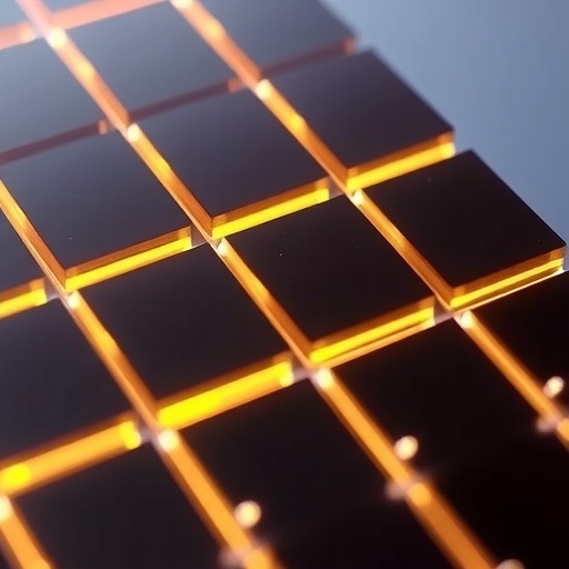
In a groundbreaking advancement that promises to redefine the landscape of renewable energy, researchers have unveiled an innovative approach to manufacturing inverted perovskite solar modules, achieving an unprecedented 99.3% geometrical fill factor through nanosecond single laser patterning. This breakthrough not only holds the potential to significantly enhance the efficiency and durability of perovskite solar cells but also marks a pivotal step toward scalable, cost-effective solar technology that could accelerate the global transition to clean energy. The study, led by Soto, Duarte, Mendes, and their colleagues, published in Communications Engineering, sheds new light on the intricate process of solar module fabrication that combines precision laser technology with cutting-edge materials science.
Perovskite solar cells, known for their remarkable light-absorbing capabilities and ease of fabrication, have long been hailed as the next big thing in photovoltaics. However, practical challenges, particularly in module scaling and the minimization of inactive areas or defects during production, have constrained their widespread commercialization. Traditional approaches to module patterning often involve multiple laser steps and complex processing sequences that introduce material loss and reduce the active area capable of harvesting sunlight. Addressing these challenges head-on, the research team developed a nanosecond single laser patterning technique that streamlines the fabrication process, preserves material integrity, and boosts the geometrical fill factor—an essential metric reflecting the proportional area of active solar material relative to the entire module surface.
The essence of the innovation lies in the utilization of ultrafast laser pulses in the nanosecond domain, which enables highly precise ablation of layers within the inverted perovskite module architecture. Unlike conventional multi-step scribing, this single-step laser process can delineate the series connection within the module without inflicting collateral damage that would degrade the perovskite layer or compromise interfaces critical for charge transport. The research reveals that this method yields remarkably consistent patterning with superior spatial resolution, allowing the modules to reach a geometrical fill factor of 99.3%, a value that is exceedingly close to an ideal scenario where almost no area is lost to inactive components or interconnection gaps.
The inverted configuration of the perovskite solar cells—where the electron transport layer is positioned below the perovskite absorber, and the hole transport layer lies on top—further complements the laser patterning approach. This architecture not only enhances device stability and operational lifespan but also facilitates the laser scribing step because of the accessible layer sequence. The interplay between the device design and the laser processing parameters was meticulously optimized, demonstrating the importance of synergistic engineering to push the boundaries of solar module efficiency and manufacturability.
By achieving a geometrical fill factor typically reserved for the most sophisticated silicon-based modules, this research bridges a critical gap between perovskite laboratory-scale devices and industrially viable solar modules. The near-complete elimination of inactive area through precise laser patterning heralds improved power conversion efficiencies since a higher proportion of incident sunlight is harnessed productively. Additionally, the process reduces wastage of expensive materials, underlying the economic advantages of this technique for large-scale solar panel manufacturing.
Beyond efficiency gains, the nanosecond single laser patterning method supports enhanced module reliability. The study highlights that the technique inflicts minimal thermal and mechanical stresses, mitigating micro-cracks, delamination, and other defects that typically plague laser-patterned solar panels. Such structural integrity leads to more robust device operation over extended periods, which is essential for the deployment of perovskite solar technologies in real-world conditions where long-term durability is critical.
The implications of this research extend to the future paradigm of solar energy deployment, especially as the world intensifies efforts to meet ambitious climate targets. The capacity to produce high-quality, cost-effective perovskite solar modules with minimal inactive areas means these technologies can compete more effectively against entrenched photovoltaic technologies. Moreover, the scalable laser patterning process could enable roll-to-roll manufacturing on flexible substrates, paving the way for innovative applications such as building-integrated photovoltaics and portable power solutions.
The authors’ exhaustive experimentation involved modulating key laser parameters such as pulse duration, energy, and scanning speed, elucidating the delicate balance between sufficient energy to ablate conductive layers while preserving the underlying perovskite. The precise control also avoided direct exposure of sensitive layers that might degrade under laser irradiation. Electrical characterization of the resulting solar modules confirmed high fill factors, low series resistance, and consistent photovoltaic performance indicators, all correlating well with the structural observations from microscopic imaging techniques.
Importantly, the research addresses a crucial bottleneck in perovskite solar cell technology: the scale-up from small, lab-scale devices to large-area modules. The demonstration of this manufacturing approach on modules rather than just single cells is a confirmation of its practical adaptability. The approach is compatible with existing module design standards and can be integrated into established production lines with minimal modification, potentially accelerating the commercialization pathway for perovskite-based photovoltaic products.
A multifaceted benefit lies in the reduced energy and resource consumption during manufacturing. The single-step laser scribing reduces processing time and complexity, leading to lower production costs and a smaller environmental footprint. This aligns well with sustainable manufacturing principles and enhances the overall lifecycle assessment profile of perovskite solar modules, making them not only efficient energy harvesters but also environmentally responsible solutions.
Thermal management considerations also play into the laser process optimization, as the nanosecond pulse duration confines heat affected zones, preventing excessive thermal diffusion that could otherwise degrade sensitive layers. This precise energy delivery mechanism ensures cleanliness and sharpness in the laser-cut pattern edges, pivotal for maintaining excellent electrical isolation between cells and avoiding leakage currents that deteriorate module performance.
Given the rapid evolution of perovskite photovoltaic technologies, this study adds a vital piece to the puzzle by providing a scalable, reliable, and high-precision manufacturing technique. Its contribution is poised to inspire further research into integrated laser processing methods for next-generation solar cells, especially as attention grows on tandem architectures that combine perovskite with silicon for even higher efficiencies.
In summary, the demonstration of inverted perovskite solar modules with an ultra-high 99.3% geometrical fill factor via nanosecond single laser patterning represents a landmark achievement. It exemplifies the power of multidisciplinary innovation, uniting materials science, laser physics, and device engineering to tackle one of the most pressing challenges in photovoltaic technology. As the world pivots to solar energy as a cornerstone of sustainable development, this work charts a promising course toward widespread adoption of cutting-edge perovskite solar modules that are efficient, durable, and economically viable.
Subject of Research: Manufacturing innovations and device architecture optimization in inverted perovskite solar modules to enhance geometrical fill factor and photovoltaic efficiency via advanced laser patterning techniques.
Article Title: Inverted perovskite solar modules with 99.3% geometrical fill factor via nanosecond single laser patterning.
Article References:
Soto, A.E.R., Duarte, V.C.M., Mendes, A. et al. Inverted perovskite solar modules with 99.3% geometrical fill factor via nanosecond single laser patterning. Commun Eng 4, 198 (2025). https://doi.org/10.1038/s44172-025-00512-4
Image Credits: AI Generated
